
Page 91 - Microsensors, MEMS and Smart Devices - Gardner Varadhan and Awadelkarim
P. 91
72 STANDARD MICROELECTRONIC TECHNOLOGIES
100
ECL
10
TTL GaAs
1 -
0.1 -
CMOS
0.01
0.001
1,000 100 10 1 0.1 0.01
Gate-switching speed (ns)
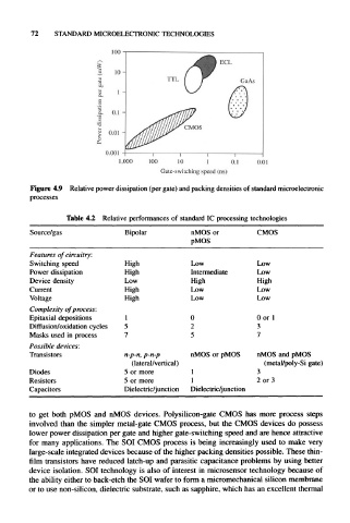
Figure 4.9 Relative power dissipation (per gate) and packing densities of standard microelectronic
processes
Table 4.2 Relative performances of standard IC processing technologies
Source/gas Bipolar nMOS or CMOS
pMOS
Features of circuitry:
Switching speed High Low Low
Power dissipation High Intermediate Low
Device density Low High High
Current High Low Low
Voltage High Low Low
Complexity of process:
Epitaxial depositions 1 0 0 or 1
Diffusion/oxidation cycles 5 2 3
Masks used in process 7 5 7
Possible devices:
Transistors n-p-n, p-n-p nMOS or pMOS nMOS and pMOS
(lateral/vertical) (metal/poly-Si gate)
Diodes 5 or more 3
Resistors 5 or more 1 2 or 3
Capacitors Dielectric/junction Dielectric/junction
to get both pMOS and nMOS devices. Polysilicon-gate CMOS has more process steps
involved than the simpler metal-gate CMOS process, but the CMOS devices do possess
lower power dissipation per gate and higher gate-switching speed and are hence attractive
for many applications. The SOI CMOS process is being increasingly used to make very
large-scale integrated devices because of the higher packing densities possible. These thin-
film transistors have reduced latch-up and parasitic capacitance problems by using better
device isolation. SOI technology is also of interest in microsensor technology because of
the ability either to back-etch the SOI wafer to form a micromechanical silicon membrane
or to use non-silicon, dielectric substrate, such as sapphire, which has an excellent thermal