
Page 86 - Microsensors, MEMS and Smart Devices - Gardner Varadhan and Awadelkarim
P. 86
WAFER PREPARATION 67
First, the boule is ground down to a standard diameter for use in the automated processing
of wafers. This is done by a variety of wheel or belt grinders with a bias of about
+0.4 mm, but it leaves a damaged surface on the crystal. The outer damaged material
is then removed later by a less harsh treatment to give the desired wafer diameter (see
following text). The standard wafer sizes vary according to the microelectronic compo-
nent that is manufactured and the desired yield. Low volume production (e.g. specialist
microsensors/MEMS fabrication) may still use a 3" 4" or 6" wafer, whereas high volume
production of memory or microprocessor chips would use the highest available diameter,
that is, 8" or higher.
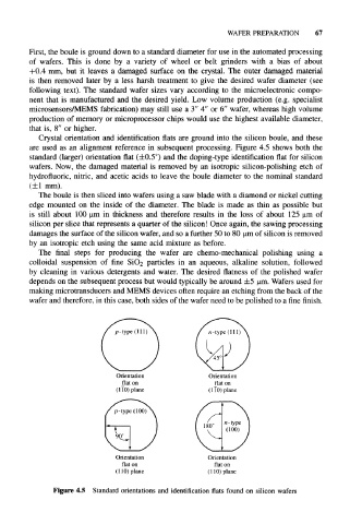
Crystal orientation and identification flats are ground into the silicon boule, and these
are used as an alignment reference in subsequent processing. Figure 4.5 shows both the
standard (larger) orientation flat (±0.5°) and the doping-type identification flat for silicon
wafers. Now, the damaged material is removed by an isotropic silicon-polishing etch of
hydrofluoric, nitric, and acetic acids to leave the boule diameter to the nominal standard
(±1 mm).
The boule is then sliced into wafers using a saw blade with a diamond or nickel cutting
edge mounted on the inside of the diameter. The blade is made as thin as possible but
is still about 100 um in thickness and therefore results in the loss of about 125 urn of
silicon per slice that represents a quarter of the silicon! Once again, the sawing processing
damages the surface of the silicon wafer, and so a further 50 to 80 um of silicon is removed
by an isotropic etch using the same acid mixture as before.
The final steps for producing the wafer are chemo-mechanical polishing using a
colloidal suspension of fine SiO 2 particles in an aqueous, alkaline solution, followed
by cleaning in various detergents and water. The desired flatness of the polished wafer
depends on the subsequent process but would typically be around ±5 urn. Wafers used for
making microtransducers and MEMS devices often require an etching from the back of the
wafer and therefore, in this case, both sides of the wafer need to be polished to a fine finish.
Orientation Orientation
flat on flat on
(110) plane (110) plane
Orientation Orientation
flat on flat on
(110) plane (110) plane
Figure 4.5 Standard orientations and identification flats found on silicon wafers