
Page 84 - Microsensors, MEMS and Smart Devices - Gardner Varadhan and Awadelkarim
P. 84
WAFER PREPARATION 65
Pull
Gas inlet Rotation
Cooled
silica
enclosure
Seed
crystal
crystal
Stirred
melt
RF power
Gas outlet
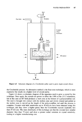
Figure 4.3 Schematic diagram of a Czochralski puller used to grow single-crystal silicon
the Czochralski process. An alternative method is the float-zone technique, which is more
expensive but results in a higher level of crystal purity.
Figure 4.4 shows a schematic diagram of the apparatus used to grow a crystal by this
technique. Once again, the crystals are grown in either the (100) or the (111) orientation,
but in this case an RF field produces a melt zone at the bottom of a polycrystalline rod.
The seed is brought into contact with the molten zone and slowly rotated and pulled as
the molten zone is moved up the length of the polycrystalline rod until the process is
k
complete. Crystals with bulk resistivities up to 30 - c m have been obtained using this
technique, and they show a higher purity than the Czochralski crystals (typically less
than 25 -cm). The main drawbacks of this technique are that the crystals have smaller
k
diameter (less than 75 mm) and show a greater radial variation in crystal resistivity,
leading to a higher manufacturing cost.