
Page 95 - Microsensors, MEMS and Smart Devices - Gardner Varadhan and Awadelkarim
P. 95
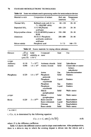
76    STANDARD MICROELECTRONIC   TECHNOLOGIES

         Table  4.4  Some wet etchants  used  in processing wafers for semiconductor devices
         Material  to etch  Composition  of etchant  Etch rate  Temperature
                                                    (nm/min)    (°C)
         Thermal  SiO2      Buffered  oxide  etch  4: 1 to  80-120  20-30
                              7:1 NH4F/HF(49%)
         Deposited  SiO2    3:3:2 NF 4F/acetic      180-220     20-30
                              acid/water
         Polycrystalline  silicon  1:50:20 HF/HNO 3/water  or  350-500  20-30
                              KOH
         Aluminum           50:10:2:3  Phosphoric   200-600     20-40
                              acid/acetic  acid/nitric
                              acid/water
         Silicon  nitride   Phosphoric  acid          5-7.5    160-175

                  Table  4.5  Source  materials  for doping  silicon  substrates

   Element       \/D  at  Solid    Compound        State    Use
                 1100°C  solubility at  name
                (um      1150°C

   n-type:
   Antimony       0.110  7xl0  1 9 a  Antimony  trioxide  Solid  Subcollector
   Arsenic        0.090  1.8 x 10 21  Arsenic  trioxide  Solid  Closed  tube or  source
                                                              furnace;
                                                              subcollector
                                   Arsine          Gas      Subcollector/emitter
   Phosphorus    0.329   1.4X10 21  Phosphoric     Solid    Emitters
                                     pentoxide
                                   Phosphoric      Liquid   Emitters
                                     oxychloride
                                   Phosphine       Gas      Emitters
                                   Phosphoric      Liquid   Emitters
                                     oxychloride
                                   Silicon         Solid    Wafer  source
                                     pyrophosphate
   p-type:                         Silicon         Solid    Wafer  source
                                     pyrophosphate
   Boron         0.329   5 x  lO 20a  Boron  trioxide  Solid  Base/isolation
                                   Boron  tribromide  Liquid  Base/isolation
                                   Diborane        Gas      Base/isolation
                                   Boron  nitride  Solid    Wafer  source
   a
    At  1250°C
   t,  C(x, t),  is determined by the following equation:

                           C(x,  t)  =  C s  erfc                        (4.8)

   where  D  is  the  diffusion  coefficient.
     Table  4.5 shows the different  sources used to dope semiconductors.  After  predeposition,
  there  is  a  drive-in  step  in  which  the  existing  dopant  is  driven  into  the  silicon  and  a