
Page 76 - Microsensors, MEMS and Smart Devices - Gardner Varadhan and Awadelkarim
P. 76
SEMICONDUCTORS 57
Table 3.7 A list of specifications for silicon wafers
Diameter Parameter 100 mm 125 mm 150 mm
Thickness (mm) 0.50-0.55 0.60-0.65 0.65-0.70
Primary flat a 30-35 40-45 55-60
length (mm)
Secondary flat 16-20 25-30 35-40
length (mm)
Bow (mm) 70 60
Total thickness 65 50
variation (u,m)
Surface orientation (100) or (111) (100) or (111) (100) or (111)
"Wafer flats are defined in Section 4.2.
from crystal growth from the melt in that the epitaxial layer can be grown at a temperature
very much below the melting point. Among various epitaxial processes, vapour-phase
epitaxy (VPE) is the usual process for silicon layer growth.
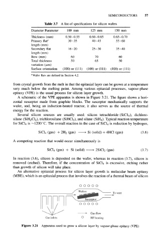
A schematic of the VPE apparatus is shown in Figure 3.21. The figure shows a hori-
zontal susceptor made from graphite blocks. The susceptor mechanically supports the
wafer, and, being an induction-heated reactor, it also serves as the source of thermal
energy for the reaction.
Several silicon sources are usually used: silicon tetrachloride (SiCl 4), dichloro-
silane (SiH 2Cl 2), trichlorosilane (SiHCl 3), and silane (SiH 4). Typical reaction temperature
for SiCl 4 is ~1200°C. The overall reaction in the case of SiCl 4 is reduction by hydrogen,
SiCl 4 (gas) + 2H 2 (gas) > Si (solid) + 4HC1 (gas) (3.6)
A competing reaction that would occur simultaneously is
(gas) + Si (solid) 2SiCl 2 (gas) (3.7)
SiCl 4
In reaction (3.6), silicon is deposited on the wafer, whereas in reaction (3.7), silicon is
removed (etched). Therefore, if the concentration of SiCl 4 is excessive, etching rather
than growth of silicon will take place.
An alternative epitaxial process for silicon layer growth is molecular beam epitaxy
(MBE), which is an epitaxial process that involves the reaction of a thermal beam of silicon
To vent
Gas flow
Gas inlets O RF heating
Figure 3.21 Apparatus used to grow a silicon layer by vapour-phase epitaxy (VPE)