
Page 75 - Microsensors, MEMS and Smart Devices - Gardner Varadhan and Awadelkarim
P. 75
56 MEMS MATERIALS AND THEIR PREPARATION
2. A crystal pulling mechanism, which is composed of a seed holder and a rotation
mechanism.
3. An atmosphere control, which includes a gas source (usually an inert gas), a flow
control, and an exhaust system.
In crystal growing, the EGS is placed in the crucible and the furnace is heated above
the melting temperature of silicon. An appropriately oriented seed crystal (e.g. [100]) is
suspended over the crucible in a seed holder. The seed is lowered into the melt. Part of
it melts but the tip of the remaining seed crystal still touches the liquid surface. The seed
is then gently withdrawn. Progressive freezing at the solid-liquid interface yields a large
single crystal. A typical pull rate is a few millimeters per minute.
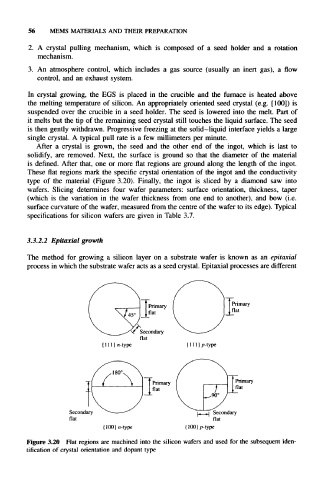
After a crystal is grown, the seed and the other end of the ingot, which is last to
solidify, are removed. Next, the surface is ground so that the diameter of the material
is defined. After that, one or more flat regions are ground along the length of the ingot.
These flat regions mark the specific crystal orientation of the ingot and the conductivity
type of the material (Figure 3.20). Finally, the ingot is sliced by a diamond saw into
wafers. Slicing determines four wafer parameters: surface orientation, thickness, taper
(which is the variation in the wafer thickness from one end to another), and bow (i.e.
surface curvature of the wafer, measured from the centre of the wafer to its edge). Typical
specifications for silicon wafers are given in Table 3.7.
3.3.2.2 Epitaxial growth
The method for growing a silicon layer on a substrate wafer is known as an epitaxial
process in which the substrate wafer acts as a seed crystal. Epitaxial processes are different
Primary
Secondary
flat
{111}n-type {111} p-type
Primary
flat
Secondary Secondary
flat flat
{100}n-type {100}/>-type
Figure 3.20 Flat regions are machined into the silicon wafers and used for the subsequent iden-
tification of crystal orientation and dopant type