
Page 71 - Microsensors, MEMS and Smart Devices - Gardner Varadhan and Awadelkarim
P. 71
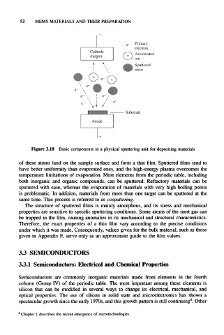
52    MEMS MATERIALS AND THEIR   PREPARATION


                                                e-  Primary
                                                    electron
                                                    Accelerated
                                               © ion
                                                    Sputtered
                                                    atom


                                                Substrate
                                   Anode


           Figure  3.18  Basic components in a physical sputtering unit  for depositing materials

      of  these  atoms  land on  the  sample  surface  and  form  a  thin film. Sputtered films tend to
      have better  uniformity  than evaporated ones,  and  the high-energy plasma  overcomes  the
      temperature  limitations  of  evaporation.  Most elements  from  the  periodic  table, including
      both  inorganic  and  organic  compounds,  can  be  sputtered.  Refractory  materials  can  be
      sputtered  with  ease,  whereas  the  evaporation  of  materials  with very  high  boiling  points
      is  problematic.  In  addition,  materials  from  more than one  target  can  be  sputtered  at  the
      same time. This process is referred to as  cosputtering.
        The  structure of  sputtered  films  is  mainly amorphous,  and  its  stress  and  mechanical
      properties  are sensitive to specific sputtering conditions. Some atoms of the inert gas can
      be trapped  in the film, causing  anomalies  in its mechanical  and structural  characteristics.
      Therefore,  the  exact  properties  of  a  thin  film  vary  according  to  the  precise  conditions
      under which it was made. Consequently, values given for the bulk material, such as those
      given  in Appendix F,  serve only as  an approximate guide to  the  film values.


      3.3  SEMICONDUCTORS

      3.3.1  Semiconductors:  Electrical  and Chemical  Properties

      Semiconductors  are  commonly  inorganic  materials  made  from  elements  in  the  fourth
      column  (Group IV)  of  the  periodic  table.  The  most  important  among these  elements  is
      silicon  that  can  be  modified  in  several  ways  to  change  its  electrical,  mechanical,  and
      optical  properties.  The  use  of  silicon  in  solid  state  and  microelectronics  has  shown  a
                                                                          6
      spectacular growth since the early  1970s, and this growth pattern is still continuing . Other
      6
       Chapter  1 describes the recent emergence of microtechnologies.