
Page 69 - Microsensors, MEMS and Smart Devices - Gardner Varadhan and Awadelkarim
P. 69
50 MEMS MATERIALS AND THEIR PREPARATION
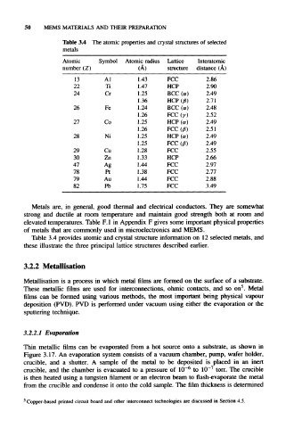
Table 3.4 The atomic properties and crystal structures of selected
metals
Atomic Symbol Atomic radius Lattice Interatomic
number (Z) (A) structure distance (A)
13 Al .43 FCC 2.86
22 Ti .47 HCP 2.90
24 Cr .25 BCC (a) 2.49
.36 HCP (ß) 2.71
26 Fe .24 BCC (a) 2.48
.26 FCC (y) 2.52
27 Co .25 HCP (a) 2.49
.26 FCC (ß) 2.51
28 Ni .25 HCP (a) 2.49
.25 FCC (ß) 2.49
29 Cu .28 FCC 2.55
30 Zn .33 HCP 2.66
47 Ag .44 FCC 2.97
78 Pt .38 FCC 2.77
79 Au .44 FCC 2.88
82 Pb .75 FCC 3.49
Metals are, in general, good thermal and electrical conductors. They are somewhat
strong and ductile at room temperature and maintain good strength both at room and
elevated temperatures. Table F.1 in Appendix F gives some important physical properties
of metals that are commonly used in microelectronics and MEMS.
Table 3.4 provides atomic and crystal structure information on 12 selected metals, and
these illustrate the three principal lattice structures described earlier.
3.2.2 Metallisation
Metallisation is a process in which metal films are formed on the surface of a substrate.
5
These metallic films are used for interconnections, ohmic contacts, and so on . Metal
films can be formed using various methods, the most important being physical vapour
deposition (PVD). PVD is performed under vacuum using either the evaporation or the
sputtering technique.
3.2.2.1 Evaporation
Thin metallic films can be evaporated from a hot source onto a substrate, as shown in
Figure 3.17. An evaporation system consists of a vacuum chamber, pump, wafer holder,
crucible, and a shutter. A sample of the metal to be deposited is placed in an inert
crucible, and the chamber is evacuated to a pressure of 10 -6 to 10 -7 torr. The crucible
is then heated using a tungsten filament or an electron beam to flash-evaporate the metal
from the crucible and condense it onto the cold sample. The film thickness is determined
5
Copper-based printed circuit board and other interconnect technologies are discussed in Section 4.5.