
Page 73 - Microsensors, MEMS and Smart Devices - Gardner Varadhan and Awadelkarim
P. 73
54 MEMS MATERIALS AND THEIR PREPARATION
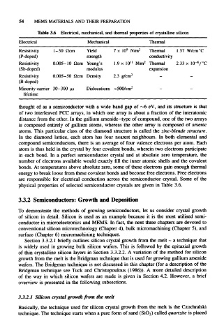
Table 3.6 Electrical, mechanical, and thermal properties of crystalline silicon
Electrical Mechanical Thermal
9 2
Resistivity 1–50 Qcm Yield 7 x 10 N/m Thermal 1.57 W/cm°C
(P-doped) strength conductivity
11
–6
Resistivity 0.005-10 Qcm Young's 1.9 x 10 N/m 2 Thermal 2.33 x 10 /°C
(Sb-doped) modulus expansion
Resistivity 0.005–50 Qcm Density 2.3 g/cm 3 - -
(B-doped)
Minority-carrier 30-300 us Dislocations <500/cm 2 — —
lifetime
thought of as a semiconductor with a wide band gap of ~6 eV, and its structure is that
of two interleaved FCC arrays, in which one array is about a fraction of the interatomic
distance from the other. In the gallium arsenide-type of compound, one of the two arrays
is composed entirely of gallium atoms, whereas the other array is composed of arsenic
atoms. This particular class of the diamond structure is called the zinc-blende structure.
In the diamond lattice, each atom has four nearest neighbours. In both elemental and
compound semiconductors, there is an average of four valence electrons per atom. Each
atom is thus held in the crystal by four covalent bonds, wherein two electrons participate
in each bond. In a perfect semiconductor crystal and at absolute zero temperature, the
number of electrons available would exactly fill the inner atomic shells and the covalent
bonds. At temperatures above absolute zero, some of these electrons gain enough thermal
energy to break loose from these covalent bonds and become free electrons. Free electrons
are responsible for electrical conduction across the semiconductor crystal. Some of the
physical properties of selected semiconductor crystals are given in Table 3.6.
3.3.2 Semiconductors: Growth and Deposition
To demonstrate the methods of growing semiconductors, let us consider crystal growth
of silicon in detail. Silicon is used as an example because it is the most utilised semi-
conductor in microelectronics and MEMS. In fact, the next three chapters are devoted to
conventional silicon microtechnology (Chapter 4), bulk micromachining (Chapter 5), and
surface (Chapter 6) micromachining techniques.
Section 3.3.2.1 briefly outlines silicon crystal growth from the melt - a technique that
is widely used in growing bulk silicon wafers. This is followed by the epitaxial growth
of thin crystalline silicon layers in Section 3.3.2.2. A variation of the method for silicon
growth from the melt is the Bridgman technique that is used for growing gallium arsenide
wafers. The Bridgman technique is not discussed in this chapter (for a description of the
Bridgman technique see Tuck and Christopoulous (1986)). A more detailed description
of the way in which silicon wafers are made is given in Section 4.2. However, a brief
overview is presented in the following subsections.
3.3.2.1 Silicon crystal growth from the melt
Basically, the technique used for silicon crystal growth from the melt is the Czochralski
technique. The technique starts when a pure form of sand (SiO 2) called quartzite is placed