Page 72 - Modern Control of DC-Based Power Systems
P. 72

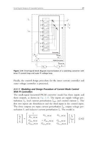
Small-Signal Analysis of Cascaded Systems                     37


                           g v ˆ           1    +              in i ˆ
                                            (s )  +
                                          _ OL
                                         Z in     +
                                        G vg  _OL (s )  + -  +  v ˆ
                                        G   (s )    + +         L i ˆ
                                         i L g  _OL   +
                          i ˆ load
                                        G ii  _OL (s )
                                        Z   (s )
                                         out  _OL
                                        G   (s )
                                          i i L  _OL
                                   d ˆ
                                        G   (s )
                                          id  _OL
                                        G   (s )
                                         vd _OL
                                        G   (s )
                                         i L d _OL
                                                 Converter
                                G c_I
                                                     T PICM
                                 +   -            PICM Converter
                                                      T PICM_FB
                                  c i ˆ
                                                  x ˆ
                                        G c_V        –1
              Figure 2.14 Small-signal block diagram representation of a switching converter with
              inner PI current loop and outer PI voltage loop.


              Finally, the control design procedure for the inner current controller and
              outer voltage controller is presented.

              2.5.1.1 Modeling and Design Procedure of Current Mode Control
              With PI Controllers
              The small-signal linearized PICM converter model has three inputs and
              three outputs, as shown in Fig. 2.15. The inputs are supply voltage per-
                                                                        ^
                                                 ^
              turbation ^ g , load current perturbation i load , and control current i c . The
                      v
              first two inputs are disturbances and the third input is the control input.
              The three outputs are input current perturbation ^ i in , output voltage per-
                      v
              turbation ^, and inductor current perturbation ^ i L . The model is
                               1
                         2                                    3
                  ^                     G ii PICM    G ic PICM
                2    3                                          2    3
                  i in                                            ^ v g
                           Z in PICM                          7
                         6
                   ^ v  5                                     7 ^        (2.42)
                4    5   6                                      4  i load  5
                           G vg PICM   2 Z out PICM  G vc PICM    ^
                         4                                    5
                   ^ i L                                          i c
                           G i L g PICM  G i L i PICM  G i L c PICM
   67   68   69   70   71   72   73   74   75   76   77