Page 74 - Modern Control of DC-Based Power Systems
P. 74

Small-Signal Analysis of Cascaded Systems                     39


                                                   T I
                                     G i L c PICM 5                      (2.51)
                                                 1 1 T I
              where T PICM 5 G c I   G i L d OL is the inner current control loop gain.
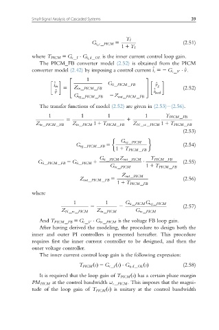
                 The PICM_FB converter model (2.52) is obtained from the PICM
                                                             ^
              converter model (2.42) by imposing a control current i c 52 G c V   ^v.
                                   1
                            2                              3
                      ^                    G ii PICM FB

                          5  4  Z in PICM FB               5             (2.52)
                      i in                                    ^ v g
                       ^ v                                    ^ i load
                              G vg PICM FB  2Z out PICM FB
                 The transfer functions of model (2.52) are given in (2.53) (2.56).
                    1            1         1              1       T PICM FB
                           5                       1
               Z in PICM FB  Z in PICM 1 1 T PICM FB  Z N vc PICM 1 1 T PICM FB
                                                                         (2.53)

                                                G vg PICM
                               G vg PICM FB 5                            (2.54)
                                               1 1 T PICM FB
                                        G ic PICM Z out PICM  T PICM FB
                G ii PICM FB 5 G ii PICM 1               U               (2.55)
                                            G vc PICM     1 1 T PICM FB
                                                 Z out PICM
                                Z out PICM FB 5                          (2.56)
                                               1 1 T PICM FB
              where
                              1            1      G ic PICM G vg PICM
                                     5          2                        (2.57)
                         Z N vc PICM   Z in PICM      G vc PICM
                 And T PICM FB 5 G c V   G vc PICM is the voltage FB loop gain.
                 After having derived the modeling, the procedure to design both the
              inner and outer PI controllers is presented hereafter. This procedure
              requires first the inner current controller to be designed, and then the
              outer voltage controller.
                 The inner current control loop gain is the following expression:
                                                                         (2.58)
                                T PICM ðsÞ 5 G c I ðsÞ  G i L d OL ðsÞ
                 It is required that the loop gain of T PICM ðsÞ has a certain phase margin
              PM PICM at the control bandwidth ω c PICM . This imposes that the magni-
              tude of the loop gain of T PICM ðsÞ is unitary at the control bandwidth
   69   70   71   72   73   74   75   76   77   78   79