Page 76 - Modern Control of DC-Based Power Systems
P. 76
Small-Signal Analysis of Cascaded Systems                     41


              2.5.1.2 Modeling and Design Procedure of Voltage Mode Control
              With PID Controller
              This procedure allows designing the voltage controller G c ðsÞ of a con-
              verter in VMC (see Fig. 2.4). The procedure is very similar to that one
              for the outer voltage controller G c V sðÞ of the converter in PICM_FB.
              Of course, the designer is required to use the proper plant transfer func-
              tion, i.e., the control-to-output transfer function G vd ðsÞ defined in (2.2).
              However, the phase of G vd ðsÞ for the basic converter topologies at high
              frequencies either approaches  180 degrees for the buck converter or
               270 degrees for the buck boost and boost converters [22]. Therefore,
              for the frequency range where the designer wants to close the voltage
              loop, there is no way with a PI control to “bump the phase up” to obtain
              a positive phase margin. The only available option is PID control. In fact,
              the derivative component of a PID control has the “phase lead effect” on
              the converter closed-loop characteristics [22]. This allows obtaining a
              positive phase margin. However, the derivative component slightly com-
              plicates the procedure to design the voltage controller since a third coeffi-
              cient needs to be found.
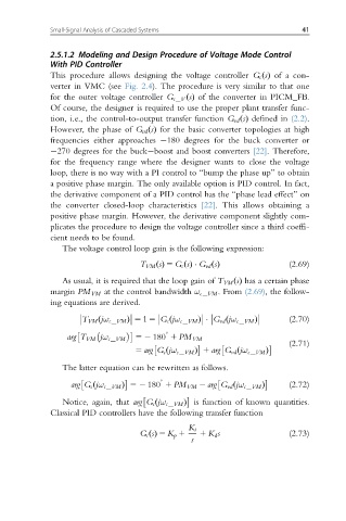
                 The voltage control loop gain is the following expression:
                                                                         (2.69)
                                    T VM ðsÞ 5 G c ðsÞ  G vd ðsÞ
                 As usual, it is required that the loop gain of T VM ðsÞ has a certain phase
              margin PM VM at the control bandwidth ω c VM .From (2.69), the follow-
              ing equations are derived.


                                                                         (2.70)
                     T VM ðjω c VM Þ 5 1 5 G c ðjω c VM Þ   G vd ðjω c VM Þ


                  arg T VM jω c VM  52 180 1 PM VM
                                                                         (2.71)

                                   5 arg G c ðjω c VM Þ 1 arg G vd ðjω c VM Þ
                 The latter equation can be rewritten as follows.


                                                                         (2.72)
                   arg G c ðjω c VM Þ 52 180 1 PM VM 2 arg G vd ðjω c VM Þ

                 Notice, again, that arg G c ðjω c VM Þ is function of known quantities.
              Classical PID controllers have the following transfer function
                                                K i
                                    G c sðÞ 5 K p 1  1 K d s             (2.73)
                                                 s

