
Page 71 - Modern Control of DC-Based Power Systems
P. 71
36 Modern Control of DC-Based Power Systems
2.5.1 Practical PI and PID Control Design
This subsection provides practical guidelines on how to design PI or PID
controllers for classical linear controls, such as VMC, CMC, and outer
voltage control for CMC or PCMC. For the converter under test, unit
gain of the voltage and current sensors and pulse-width modulator are
assumed for simplicity. The control design is performed in the s-domain,
and no digital delays are taken into account. The idea is to provide the
reader with a straightforward procedure to design basic linear controllers
that is easily implementable in programming and simulation environments
such as MATLAB and Simulink. The reader can refer to [21] if interested
in a more formal digital control design procedure that includes all the
effects that are here neglected. The reader will learn how to design PI
and PID controllers to achieve the desired dynamic behavior and a null
steady-state error. These specifications are translated into the desired con-
trol bandwidth (or crossover frequency) and phase margin of the equivalent
closed-loop system. First, the CMC with its outer voltage loop design
procedure is provided. Then, the VMC is given.
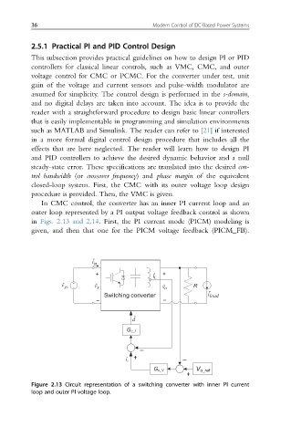
In CMC control, the converter has an inner PI current loop and an
outer loop represented by a PI output voltage feedback control as shown
in Figs. 2.13 and 2.14. First, the PI current mode (PICM) modeling is
given, and then that one for the PICM voltage feedback (PICM_FB).
in i ˆ
+ +
L i ˆ
v ˆ gs g v ˆ o v ˆ R
Switching converter i ˆ load
– –
d ˆ
G c_I
–
c i ˆ + –
G c_V V o_ref
+
Figure 2.13 Circuit representation of a switching converter with inner PI current
loop and outer PI voltage loop.