
Page 61 - Multifunctional Photocatalytic Materials for Energy
P. 61
50 Multifunctional Photocatalytic Materials for Energy
4.2 Electronic energy band structure of semiconductors
A thorough exploration of this topic involves principles of solid physics and quantum
mechanics that are beyond the scope of this chapter. Readers are strongly encouraged
to refer to professional books in these fields. The objective of this section is to briefly
present basic information on the electronic energy band structure of a semiconductor.
4.2.1 Electronic energy band of semiconductors
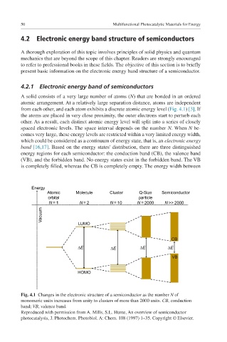
A solid consists of a very large number of atoms (N) that are bonded in an ordered
atomic arrangement. At a relatively large separation distance, atoms are independent
from each other, and each atom exhibits a discrete atomic energy level (Fig. 4.1) [3]. If
the atoms are placed in very close proximity, the outer electrons start to perturb each
other. As a result, each distinct atomic energy level will split into a series of closely
spaced electronic levels. The space interval depends on the number N. When N be-
comes very large, these energy levels are restricted within a very limited energy width,
which could be considered as a continuum of energy state, that is, an electronic energy
band [16,17]. Based on the energy states' distribution, there are three distinguished
energy regions for each semiconductor: the conduction band (CB), the valence band
(VB), and the forbidden band. No energy states exist in the forbidden band. The VB
is completely filled, whereas the CB is completely empty. The energy width between
Energy
Atomic Molecule Cluster Q-Size Semiconductor
orbital particle
N = 1 N = 2 N = 10 N = 2000 N >> 2000
Vacuum
LUMO
CB
DE DE DE DE
VB
HOMO
Fig. 4.1 Changes in the electronic structure of a semiconductor as the number N of
monomeric units increases from unity to clusters of more than 2000 units. CB, conduction
band; VB, valence band.
Reproduced with permission from A. Mills, S.L. Hunte, An overview of semiconductor
photocatalysis, J. Photochem. Photobiol. A: Chem. 108 (1997) 1–35. Copyright © Elsevier.