
Page 265 - Book Hosokawa Nanoparticle Technology Handbook
P. 265
FUNDAMENTALS CH. 4 CONTROL OF NANOSTRUCTURE OF MATERIALS
of -Al O and PZT exceeds 3 MV/cm and 500
2
3
kV/cm, respectively. Such electrical characteristics
can be useful for developing devices such as electro-
static chucks [9]. Although PZT layers deposited at
room temperature exhibit piezoelectric and ferroelec-
tric behavior, their properties are unacceptable for
practical applications because of structural defects
introduced during deposition. By post-annealing in
air at temperatures ranging from 500–600 C, grain
growth of fine crystals and defect recovery in AD
layers has been observed, dramatically improving fer-
roelectric properties. The dielectric constant ( ) and
piezoelectric constant (d ) of post-annealed layers
31
formed at 600 C were 800–1,200 and –100 pm/V as
shown in Fig. 4.5.30 [10], respectively, which is
comparable to that achieved with conventional thin-
film formation methods. Moreover, the electrical
breakdown ( 1 MV/cm) and Young’s module ( 80
GPa) of AD films exceeded those obtained with
conventional thick-film formation technology. By
post annealing at 850 C, remnant polarization (Pr) of
2
38
C/cm and coercive field strengths (E ) of
c
30 kV/cm were obtained in the PZT films [11]. Even
without adding special additives to the feed particles
or using special procedures, compared to conven-
tional screen-printing methods, the AD method
permits a 300–400? reduction of the process temper-
ature. For films deposited by using both conventional
and AD processes, Fig. 4.5.31 shows the effect on
electrical properties of heat treating films. For both
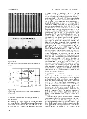
Figure 4.5.29 conventional-bulk and thin-film processes, heat
Micropatterning of PZT thick film by mask deposition treatment at more than 600 C was required to obtain
method. crystallization and densification of the films. The
most important characteristic of the AD method is
that compared to the properties of bulk materials at
room temperature, the As-deposited film has a more
dense, crystallized structure.
5. Application to MEMS devices
Because piezoelectric materials act both as sensors
and as actuators, they have a wide range of potential
application, such as ink-jet printers, high-speed actu-
ators for nanopositioning, and micro, ultrasonic
devices. To realize integrated microdevices with
piezoelectric materials, thin-film deposition technolo-
gies and associated microfabrication methods are
being actively studied in the research fields of micro
electro mechanical systems (MEMS) and micro total
Figure 4.5.30 analysis systems (
-TAS). The required thickness of
Piezoelectric constants of PZT thick film deposited by piezoelectric films for these applications is from 1 to
AD method. about 100
m (this thickness range is called “thick
films”).
Resonance type optical microscanners have been
4. Electrical properties and recovering properties by
made as one practical application of the AD film-
heat treatment formation method [12, 13]. These types of optical
As-deposited AD layers deposited at room tempera- scanners are expected to be a key component in future
ture generally have thermal insulation and electrical laser displays and retina projection-type displays. For
breakdown characteristics that exceed that of the such applications the requirements are scanning fre-
bulk material. For example, the electrical breakdown quency greater than about 30 kHz, scanning angle
240