
Page 264 - Book Hosokawa Nanoparticle Technology Handbook
P. 264
4.5 STRUCTURE CONTROL OF NANOPARTICLE COLLECTIVES BY SINTERING AND BONDING FUNDAMENTALS
increasing carrier gas flow rate, which increased the
deposition efficiency. The deposition efficiency was
also strongly affected by properties of the starting
particles, such as the average particle size and size
distribution, and mechanical and surface properties
[6]. The deposition efficiency of the AD method is
about 30 times higher than conventional thin-film-
formation methods such as sputtering, which have a
deposition rate of only about 10 nm/min for an area
2
of 5 cm . Therefore, the AD method is attractive for
manufacturing processes because it permits high
throughput.
In conventional thin-film and thermal spray-coating
methods, surface cleaning before deposition is needed
to achieve acceptable adhesion with a substrate. On
the other hand, the AD method does not require such
pre-cleaning, because during the initial stage of parti-
cle impaction with the surface, similar to sand-blasting
processes, surface contaminants such as dirt and oils
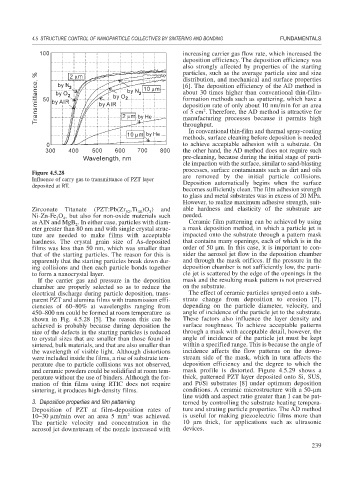
Figure 4.5.28
Influence of carry gas to transmittance of PZT layer are removed by the initial particle collisions.
deposited at RT. Deposition automatically begins when the surface
becomes sufficiently clean. The film adhesion strength
to glass and metal substrates was in excess of 20 MPa.
However, to realize maximum adhesive strength, suit-
Zirconate Titanate (PZT:Pb(Zr ,Ti )O ) and able hardness and elasticity of the substrate are
3
52
48
Ni-Zn-Fe O , but also for non-oxide materials such needed.
3
4
as AlN and MgB . In either case, particles with diam- Ceramic film patterning can be achieved by using
2
eter greater than 80 nm and with single crystal struc- a mask deposition method, in which a particle jet is
ture are needed to make films with acceptable impacted onto the substrate through a pattern mask
hardness. The crystal grain size of As-deposited that contains many openings, each of which is in the
films was less than 50 nm, which was smaller than order of 50
m. In this case, it is important to con-
that of the starting particles. The reason for this is sider the aerosol jet flow in the deposition chamber
apparently that the starting particles break down dur- and through the mask orifices. If the pressure in the
ing collisions and then each particle bonds together deposition chamber is not sufficiently low, the parti-
to form a nanocrystal layer. cle jet is scattered by the edge of the openings in the
If the carrier gas and pressure in the deposition mask and the resulting mask pattern is not preserved
chamber are properly selected so as to reduce the on the substrate.
electrical discharge during particle deposition, trans- The effect of ceramic particles sprayed onto a sub-
parent PZT and alumina films with transmission effi- strate change from deposition to erosion [7],
ciencies of 60–80% at wavelengths ranging from depending on the particle diameter, velocity, and
450–800 nm could be formed at room temperature as angle of incidence of the particle jet to the substrate.
shown in Fig. 4.5.28 [5]. The reason this can be These factors also influence the layer density and
achieved is probably because during deposition the surface roughness. To achieve acceptable patterns
size of the defects in the starting particles is reduced through a mask with acceptable detail, however, the
to crystal sizes that are smaller than those found in angle of incidence of the particle jet must be kept
sintered, bulk materials, and that are also smaller than within a specified range. This is because the angle of
the wavelength of visible light. Although distortions incidence affects the flow patterns on the down-
were included inside the films, a rise of substrate tem- stream side of the mask, which in turn affects the
perature due to particle collisions was not observed, deposition efficiency and the degree to which the
and ceramic powders could be solidified at room tem- mask profile is distorted. Figure 4.5.29 shows a
perature without the use of binders. Although the for- thick, patterned PZT layer deposited onto Si, SUS,
mation of thin films using RTIC does not require and Pt/Si substrates [8] under optimum deposition
sintering, it produces high-density films. conditions. A ceramic microstructure with a 50-
m
line width and aspect ratio greater than 1 can be pat-
3. Deposition properties and film patterning terned by controlling the substrate heating tempera-
Deposition of PZT at film-deposition rates of ture and strating particle properties. The AD method
2
10–30
m/min over an area 5 mm was achieved. is useful for making piezoelectric films more than
The particle velocity and concentration in the 10
m thick, for applications such as ultrasonic
aerosol jet downstream of the nozzle increased with devices.
239