
Page 263 - Book Hosokawa Nanoparticle Technology Handbook
P. 263
FUNDAMENTALS CH. 4 CONTROL OF NANOSTRUCTURE OF MATERIALS
Table 4.5.2 with crystal size less than 20 nm. TEM and electron
Typical deposition condition. diffraction imaging did not show either amorphous
layers or heterostructures at the boundary of crystal
Pressure in deposition grains. XRD profiles confirmed that the spectral
chamber (operation) 0.4 2 Torr phases of the -Al O particles were retained in the
3
2
Pressure in aerosol chamber 80 600 Torr deposited layer. However, broadening of the spectra
Size of nozzle orifice 5 0.3 mm 2 and a slight shifting of the spectral angle were
10 0.4 mm 2 observed. The reason for the change between the
Accelerated carry gas He, Air, N2 spectra of the particles and the deposited layer may be
Consumption of due to reduction of the film crystal size or distortion
accelerated carry gas 1 8 l /min during deposition. Clear lattice images in crystal
Substrate heating Non grains less than 10 nm were observed, as well as uni-
Relative scanning speed form microstructures at the boundary between the
of nozzle motion along substrate 0.125~1.25mm/sec substrate and the deposited layer. For -Al O layers
3
2
Distance between nozzle deposited at room temperature, film density was over
and substrate 1 20 mm 95% of theoretical density and Vickers hardness was
over 1,600 Hv. Such -Al O layers are acceptable for
3
2
use as abrasion–resistant coatings [4]. The layer hard-
without the need for high-temperature heat treatment. ness increased with increasing particle-impact veloc-
We call this process room temperature impact consol- ity, and sometimes was higher than that of the bulk
idation (RTIC) [2, 3]. material, which was sintered at a high temperature.
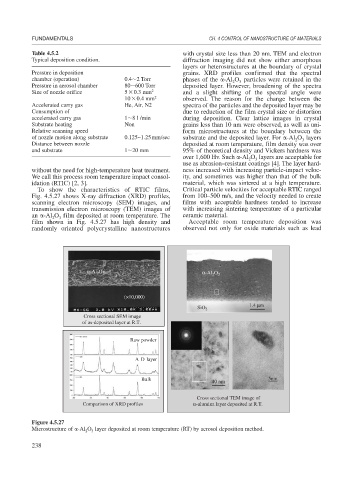
To show the characteristics of RTIC films, Critical particle velocities for acceptable RTIC ranged
Fig. 4.5.27 shows X-ray diffraction (XRD) profiles, from 100–500 m/s, and the velocity needed to create
scanning electron microscopy (SEM) images, and films with acceptable hardness tended to increase
transmission electron microscopy (TEM) images of with increasing sintering temperature of a particular
an -Al O film deposited at room temperature. The ceramic material.
2
3
film shown in Fig. 4.5.27 has high density and Acceptable room temperature deposition was
randomly oriented polycrystalline nanostructures observed not only for oxide materials such as lead
O
α-Al 2 3 α-Al O
2 3
(×10,000)
1.4 μm
SiO 2
Cross sectional SEM image
of as-deposited layer at R.T.
Raw powder
A D layer
Bulk 5nm
40 nm
Cross sectional TEM image of
Comparison of XRD profiles α-alumina layer deposited at R.T.
Figure 4.5.27
Microstructure of -Al O layer deposited at room temperature (RT) by aerosol deposition method.
2
3
238