
Page 266 - Book Hosokawa Nanoparticle Technology Handbook
P. 266
4.5 STRUCTURE CONTROL OF NANOPARTICLE COLLECTIVES BY SINTERING AND BONDING FUNDAMENTALS
Bulk properties
100%
Electrical Properties 55% Aerosol Deposition Method Low Temperature Sintering
Conventional Sintering
Conventional Thin Film Method
densification
(PVD, CSD)
densification
crystallization
crystallization densification
100 200 300 400 500 600 700 800 900 1000 1100 1200 1300
Process Temperature (°C)
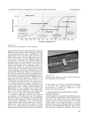
Figure 4.5.31
Recovering electrical properties by heat treatment.
greater than 20 , mirrors sufficiently large to prevent
distortion, and reduction of drive voltage. It is thought
that piezoelectric films will be desirable for such
applications because of their simple structure and Si mirror
high actuation force. However, these devices are dif- PZT cantilevers
ficult to make using conventional thin-film deposition
technologies combined with MEMS fabrication
processes, because of low deposition rates and com-
plicated etching processes. Figure 4.5.32 shows an
optical microscanner and an enlarged image of a
piezoelectric actuator. To make this devise, first the
scanner structure was made by using conventional Si Si cantilever
micromachining, and then the AD method was used to
deposit a thick PZT layer. This layer was formed on an
Si cantilever without any damage or deformation to
the cantilever from the particle impingement associ- Figure 4.5.32
ated with the AD method. Proper alignment of the Resonance type optical microscanner driven by PZT thick
mask prevented either adhesion or stacking of raw layer fabricated with AD method.
PZT particles on the mirror part. The mirror was not
influenced by the deposited film. The maximum mir-
ror scanning angle and resonance frequency in air
were 26 and 33 kHz, respectively, representing high- of this actuator was 25 mm at a resonance frequency
speed performance. Neither mirror bending nor of 22.4 kHz and a driving voltage of 8 V. This
deformation of the scanning laser beam were performance is suitable for applications using
observed by the thick structure of the microscanner micromixers and micropumps.
device. This scanner performance was higher than 6. Future prospects for using AD methods in material
that of scanners made with conventional methods.
In addition, diaphragm actuators [14] used for integration technology
micropumps can be made from thin Si membranes The AD method is a non-thermal equilibrium process,
deposited with the AD method and micromachined. which solidifies feed particles at room temperature to
These have flat frequency response and good sym- form films. This differs from thermal spray coating
metrical elastic deformation over a wide frequency methods, which use higher temperatures for film dep-
range. During fatigue testing (stability of long-time osition. There are two important features of the AD
performance) under high driving electrical fields, method. One is that the AD deposition rate is higher
there was no de-polarization nor peeling of the AD than that of conventional thin-film processes, because
deposited film from the substrate [11]. The amplitude the deposition material is particles, which carry
241