
Page 339 - Book Hosokawa Nanoparticle Technology Handbook
P. 339
FUNDAMENTALS CH. 5 CHARACTERIZATION METHODS FOR NANOSTRUCTURE OF MATERIALS
Figure 5.6.3
Dependence of electron mobility of ZnO thin films on the
grain size.
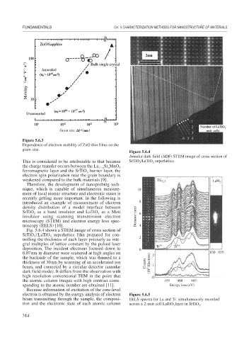
Figure 5.6.4
Annular dark field (ADF) STEM image of cross section of
This is considered to be attributable to that because SrTiO /LaTiO superlattice.
3
3
the charge transfer occurs between the La 1 x Sr MnO 3
x
ferromagnetic layer and the SrTiO barrier layer, the
3
electron spin polarization near the grain boundary is
weakened compared to the bulk materials [9]. TiL 2,3 LaM 5
Therefore, the development of nanoprobing tech-
nique, which is capable of simultaneous measure- 10
ment of local atomic structure and electronic states is
recently getting more important. In the following is
introduced an example of measurement of electron 8
density distribution of a model interface between
SrTiO as a band insulator and LaTiO as a Mott 6
3
3
insulator using scanning transmission electron Distance (nm)
microscopy (STEM) and electron energy loss spec-
troscopy (EELS) [10]. 4
Fig. 5.6.4 shows a STEM image of cross section of
SrTiO /LaTiO superlattice film prepared for con- 2
3
3
trolling the thickness of each layer precisely as inte-
gral multiples of lattice constant by the pulsed laser Ti 3+ Ti 4+
deposition. The incident electrons focused down to 0
0.07nm in diameter were scattered at high angles on 2 830 835
the backside of the sample, which was thinned to a
thickness of 30nm by scanning of an accelerated ion Counts (10 3 Electron) 1
beam, and corrected by a circular detector (annular
dark field mode). It differs from the observation with
high resolution conventional TEM in the point that 0
the atomic column images with high contrast corre- 455 460 465
sponding to the atomic number are obtained [11]. Energy loss (eV)
Because information of excitation of the core-level
electron is obtained by the energy analysis of electron Figure 5.6.5
beam transmitting through the sample, the composi- EELS spectra for La and Ti simultaneously recorded
tion and the electronic state of each atomic column across a 2-unit-cell LaTiO layer in SrTiO .
3 3
314