
Page 337 - Book Hosokawa Nanoparticle Technology Handbook
P. 337
FUNDAMENTALS CH. 5 CHARACTERIZATION METHODS FOR NANOSTRUCTURE OF MATERIALS
size from a few tens to hundreds of nm [4]. Fig. 5.6.1
shows the growth mechanism schematically. The
crystal nuclei generated on the substrate surface at the
initial stage grow along the surface keeping the crys-
tal orientation against the substrate by the domain
matching epitaxy [5] with the coinciding common
multiplier of lattice constant of the substrate and the
thin film. As the crystal lattices are not always con-
nected coherently on the coalescence of crystal
grains, incoherent grain boundaries occur.
The incompleteness of crystallinity in the real
space of nanostructure having grown in this way and
expansion of diffraction peaks in the reciprocal space
are explained in Fig. 5.6.2. Considering the crystallo-
graphic tilting and the in-plane average size of the
grains (average distance between the coherent grain
boundaries) as a measure of the incompleteness of
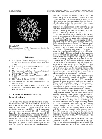
Figure 5.5.17
Reconstructed image of TiO –Ag composites, showing the crystalline, they give diffused pattern to all the dif-
2
distribution of Ag particles [7]. fraction spots. Focusing on a plane in the reciprocal
space, the crystallographic tilting gives the diffraction
peak circularly diffused vertical to the reciprocal
space vector and the finite grain size gives diffused
spread in the direction parallel to the plane, of which
References
width is inversely proportional to grain size. As seen
[1] R.F. Egerton: Electron Energy-Loss Spectroscopy in from Fig. 5.6.2a, these spread directions overlap on
the Electron Microscope, Plenum Press, New York the diffraction of the symmetric plane but meet at an
(1996). angle with the asymmetric faces. Therefore it is pos-
sible to measure the width of the crystallographic tilt-
[2] D.D. Vvedensky, D.K. Saldin and J.B. Pendry: Comput.
ing of crystal grains and the grain size independently
Phys. Commun., 40, 421–440 (1986).
by measuring the reciprocal space mapping of an
[3] J.C. Fuggle, J.E. Inglesfield: Unoccupied Electronic
asymmetric plane and dividing the spread width of
States, Springer-Verlag, Berlin (1992).
diffraction spots in the individual directions.
[4] J. Bruley: Microsc. Micronanal. Microstruct., 4, 23–39 The evaluation of the structure of nanocrystalline
(1993). film by this method is a very simple and direct method
[5] J.M. Titchmarsh: Micron, 30, 159–171 (1999). without using the etching method or TEM observation.
[6] P.A. Midgley, M. Weyland: Ultramicroscopy, 96, Besides, it can evaluate the grain size as small as
413–451 (2003). 10 nm, which is out of the range of X-ray topography.
[7] K. Kaneko, W.J. Moon, K. Inoke, Z. Horita, S. Ohara, Actually, this method is reported to be useful for the
investigation of grain boundary scattering of conduc-
T. Adschiri, H. Abe and M. Naito, Mater. Sci. Eng. A,
tion electrons in the ZnO nanocrystalline films [6].
403, 30–36 (2005).
Fig. 5.6.3 shows the dependence of electron mobility
on the grain size in ZnO thin film grown on the c-plane
5.6 Evaluation methods for oxide sapphire substrate under various preparation condi-
tions. It is seen that the electron mobility decreases
heterostructures
with the decreasing size because the double Schottky
barrier formed due to deep level electrons trapped in
Two recent technologies for the evaluation of oxide the grain boundaries acts as major scattering centers
heterostructures will be introduced in this section. electronic conduction. After annealing, the mobility
First a method to measure the in-plane grain size of becomes independent of the grain size because the
ZnO epitaxial layer [1], which is expected to be effect of Schottky barrier becomes weak in terms of
applied for an ultra-violet LED, by the X-ray recipro- both the larger grain size and higher electron density.
cal space mapping method [2] will be explained. The relationship between the grain size and electric
Secondly, the nanoprobe measuring method [3] properties is relavant to the operating characteristics of
applied for evaluation of local electronic structure of transparent transistors using ZnO polycrystalline film
the artificial superlattice consisting of perovskite as a channel [7].
oxides will be briefly described. In the epitaxial An interesting phenomenon has been found con-
growth of the system with large lattice mismatch like cerning the incoherent grain boundary in ZnO thin
ZnO thin film on the c-plane sapphire substrate, the film that it works as a cavity of laser emission [4]. The
thin film grows by coalescence of crystal grains of a reciprocal space mapping with high resolution optics
312