
Page 333 - Book Hosokawa Nanoparticle Technology Handbook
P. 333
FUNDAMENTALS CH. 5 CHARACTERIZATION METHODS FOR NANOSTRUCTURE OF MATERIALS
In the case of using a small electron probe for near-edge fine structure. Although point analysis by
acquiring EDS signals, it usually causes the irradia- parallel-detection EEL spectrometer was mainstream in
tion damage on the specimen during the acquisition. past, energy-filtering TEM (EF-TEM) became the stan-
dard method recently with advances of methods and
5.5.2.2 Electron energy-loss spectroscopy (EELS) equipments.
Collisions of incident electrons with the specimen can
be classified into three types of scatterings, unscattered, Comparison of EELS and EDXS
elastically or inelastically scattered, as illustrated in
Fig. 5.5.3. If incident electrons suffer collisions result- EELS EDXS
ing in energy transfer, the energy transferred to the
specimen must be measured for achieving information High detection efficiency High detection efficiency
of the specimen. In practice, electron trajectories are for low Z elements for high Z elements
bent by magnetic prisms; the trajectories of electrons Elemental, chemical, and Elemental information only
which suffered inelastic collisions are bent more than dielectric information
those which interacted with the specimen elastically. In Energy resolution 0.3–2 eV Energy resolution
100 eV
other words the electrons are dispersed according to results in far fewer overlaps; causes frequent overlaps
their amount of energy loss. A photodiode array can be fine structures can be
used to detect the different trajectories of the electrons analyzed
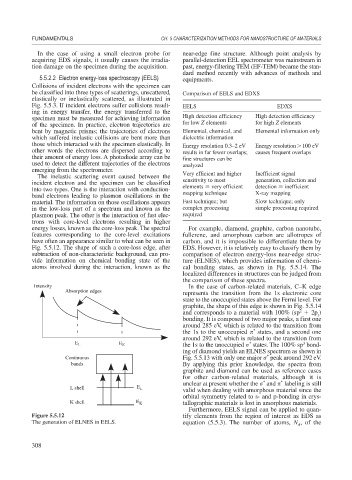
emerging from the spectrometer. Very efficient and higher Inefficient signal
The inelastic scattering event caused between the
incident electron and the specimen can be classified sensitivity to most generation, collection and
elements very efficient
detection inefficient
into two types. One is the interaction with conduction- mapping technique X-ray mapping
band electrons leading to plasmon oscillations in the
material. The information on those oscillations appears Fast technique; but Slow technique; only
in the low-loss part of a spectrum and known as the complex processing simple processing required
plasmon peak. The other is the interaction of fast elec- required
trons with core-level electrons resulting in higher
energy losses, known as the core-loss peak. The spectral For example, diamond, graphite, carbon nanotube,
features corresponding to the core-level excitations fullerene, and amorphous carbon are allotropes of
have often an appearance similar to what can be seen in carbon, and it is impossible to differentiate them by
Fig. 5.5.12. The shape of such a core-loss edge, after EDS. However, it is relatively easy to classify them by
subtraction of non-characteristic background, can pro- comparison of electron energy-loss near-edge struc-
vide information on chemical bonding state of the ture (ELNES), which provides information of chemi-
atoms involved during the interaction, known as the cal bonding states, as shown in Fig. 5.5.14. The
localized differences in structures can be judged from
the comparison of these spectra.
Intensity In the case of carbon-related materials, C–K edge
Absorption edges represents the transition from the 1s electronic core
state to the unoccupied states above the Fermi level. For
graphite, the shape of this edge is shown in Fig. 5.5.14
and corresponds to a material with 100% (sp 2p )
2
z
bonding. It is composed of two major peaks, a first one
around 285 eV, which is related to the transition from
*
the 1s to the unoccupied states, and a second one
around 292 eV, which is related to the transition from
E
*
3
E L K the 1s to the unoccupied
states. The 100% sp bond-
ing of diamond yields an ELNES spectrum as shown in
*
Continuous Fig. 5.5.13 with only one major
peak around 292 eV.
bands By applying this prior knowledge, the spectra from
graphite and diamond can be used as reference cases
for other carbon-related materials, although it is
*
unclear at present whether the
and labeling is still
*
L shell E L valid when dealing with amorphous material since the
orbital symmetry related to s- and p-bonding in crys-
K shell E K tallographic materials is lost in amorphous materials.
Furthermore, EELS signal can be applied to quan-
Figure 5.5.12 tify elements from the region of interest as EDS as
The generation of ELNES in EELS. equation (5.5.3). The number of atoms, N , of the
A
308