
Page 328 - Book Hosokawa Nanoparticle Technology Handbook
P. 328
5.5 GRAIN BOUNDARIES AND INTERFACES FUNDAMENTALS
References
[1] G. Horvath, K. Kawazoe: J. Chem. Eng. Jpn., 16,
470–475 (1983).
[2] A. Saito, H.C. Foley: AIChE J., 37, 429–436 (1991).
[3] S. Kondo, T. Ishikawa and I. Abe: Kyuchaku no
Kagaku (Science of Adsorption), Maruzen Publishing,
Tokyo, pp. 31–83 (1991).
[4] M. Senoo, ed.: Koroido Kagaku IV – Koroido Kagaku
Jikkenhou (Colloid Chemistry – Experimental Method
for Colloid Chemistry), edited by Japan Society of
Chemistry, Tokyo Kagaku Dojin, Tokyo, pp. 289–296
(1996).
[5] R.W. Cranston, F.A. Inkley: Adv. Catal., 9, 143–154
(1957).
[6] D. Dollimore, G.R. Heal: J. Appl. Chem., 14, 109–114
(1964).
[7] E.P. Barell, L.G. Joyner and P.P. Halenda: J. Am.
Chem. Soc., 73, 373–380 (1951).
[8] R. Evans, U.M.B. Marconi and P. Tarazona: J. Chem.
Phys., 84, 2376–2399 (1986).
[9] M. Miyahara, T. Yoshioka and M. Okazaki: J. Chem.
Phys., 106, 8124–8134 (1997).
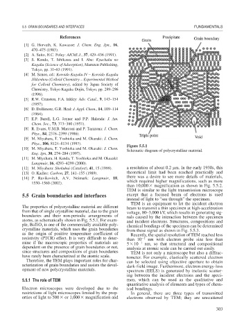
Figure 5.5.1
[10] M. Miyahara, T. Yoshioka and M. Okazaki: J. Chem.
Schematic diagram of polycrystalline material.
Eng. Jpn, 30, 274–284 (1997).
[11] M. Miyahara, H. Kanda, T. Yoshioka and M. Okazaki:
Langmuir, 16, 4293–4299 (2000).
[12] M. Miyahara: Shokubai (Catalyst), 41, 15 (1999). a resolution of about 0.2 m. In the early 1930s, this
[13] O. Kadlec: Carbon, 27, 141–155 (1989). theoretical limit had been reached practically and
there was a desire to see more details of materials,
[14] P. Ravikovitch, A.V. Neimark: Langmuir, 18,
which required higher magnifications, such as more
1550–1560 (2002).
than 10,000 magnification as shown in Fig. 5.5.2.
TEM is similar to the light transmission microscope
5.5 Grain boundaries and interfaces except that a focused beam of electrons is used
instead of light to “see through” the specimen.
TEM is an equipment to let the incident electron
The properties of polycrystalline material are different beam to transmit a thin specimen at high-acceleration
from that of single crystalline material, due to the grain voltage, 80–3,000 kV, which results in generating sig-
boundaries and their non-periodic arrangements of nals caused by the interaction between the specimen
atoms, as schematically shown in Fig. 5.5.1. For exam- and incident electrons. Structures, compositions and
ple, BaTiO is one of the commercially available poly- chemical bondings of the specimen can be determined
3
crystalline materials, which uses the grain boundaries from these signal as shown in Fig. 5.5.3.
as the origin of positive temperature coefficient of Recently, the spatial resolution of TEM reached less
resistivity (PTCR) effect. It is very difficult to deter- than 10 1 nm with electron probe size less than
mine if the macroscopic properties of materials are 5 10 1 nm, so that structural and compositional
dependent on the presence of grain boundaries or not, analysis at atomic scale can be carried out easily.
since structures and compositions of grain boundaries TEM is not only a microscope but also a diffrac-
have rarely been characterized at the atomic scale. tometer. For example, elastically scattered electron
Therefore, the TEM plays important roles for char- can be selected using objective aperture to obtain
acterization of grain boundaries and assists the devel- dark-field image. Furthermore, electron energy-loss
opment of new polycrystalline materials. spectrum (EELS) is generated by inelastic scatter-
ing between the incident electrons and the speci-
5.5.1 The role of TEM men, which can be used as the qualitative and
quantitative analysis of elements and types of chem-
Electron microscopes were developed due to the ical bondings.
restrictions of light microscopes limited by the prop- In general, there are three types of transmitted
erties of light to 500 or 1,000 magnification and electrons observed by TEM; they are unscattered
303