
Page 331 - Book Hosokawa Nanoparticle Technology Handbook
P. 331
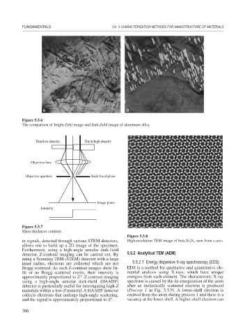
FUNDAMENTALS                            CH. 5 CHARACTERIZATION METHODS FOR NANOSTRUCTURE OF MATERIALS


                  Figure 5.5.6
                  The comparison of bright-field image and dark-field image of aluminum alloy.


                        Thin/low density     Thick/high density


                      Objective lens


                   Objective aperture            Back focal plane


                                                   Image plane
                          Intensity


                  Figure 5.5.7
                  Mass-thickness contrast.
                                                                 Figure 5.5.8
                  in signals, detected through various STEM detectors,  High-resolution TEM image of beta Si N seen from c-axis.
                                                                                              4
                                                                                            3
                  allows one to build up a 2D image of the specimen.
                  Furthermore, using a high-angle annular dark-field
                  detector, Z-contrast imaging can be carried out. By  5.5.2 Analytical TEM (AEM)
                  using a Scanning TEM (STEM) detector with a large
                  inner radius, electrons are collected which are not  5.5.2.1 Energy dispersive X-ray spectroscopy (EDS)
                  Bragg scattered. As such Z-contrast images show lit-  EDS is a method for qualitative and quantitative ele-
                  tle or no Bragg scattered events, their intensity is  mental analysis using X-rays, which have unique
                                            2
                  approximately proportional to Z . Z-contrast imaging  energies from each element. The characteristic X-ray
                  using a high-angle annular dark-field (HAADF)  spectrum is caused by the de-energization of the atom
                  detector is particularly useful for investigating high-Z  after an inelastically scattered electron is produced
                  materials within a low-Z material. A HAADF detector  (Process 1 in Fig. 5.5.9). A lower-shell electron is
                  collects electrons that undergo high-angle scattering,  emitted from the atom during process 1 and there is a
                                                         2
                  and the signal is approximately proportional to Z .   vacancy at the lower shell. A higher-shell electron can
                  306