
Page 334 - Book Hosokawa Nanoparticle Technology Handbook
P. 334
5.5 GRAIN BOUNDARIES AND INTERFACES FUNDAMENTALS
element analyzed can be quantified by equation
(5.5.3) using EELS signal [1].
I (, E E ) 1
,
N A 0 (5.5.3)
(,
A
I t t
E E )
,
A
0
I is the total incident electron current, I the number
t
A
of electron having excited kth inner shell from ele-
ment A, t the specimen thickness, the collection
angle, E the energy slit width, E the energy of
0
entering electron, and
(t, E, E ) an ionization cross-
0
section for the kth shell of element A. Furthermore,
the ratio N /N can be obtained from equation (5.5.4).
B
A
(,
N A I (, E E , 0 )
EE , 0 )
B
A
(,
N B I (, E E , 0 )
EE , 0 ) (5.5.4)
B
A
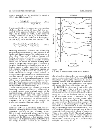
Predicting theoretical reference and identifying
ELNES-structure correlation, ELNES is related to the
local chemical environment of the excited atom and is
often called “fingerprint” to indicate chemical and
bonding information of materials. From the compari-
son between acquired spectra and available reference
spectra, one can deduce the chemical bonding infor-
mation of the specimen. For example, a fine structure
2
in carbon K-edge can be used to identify the sp or sp 3
bonding nature in carbon materials by comparison
with available reference experimental spectra, as Figure 5.5.13
shown in Fig. 5.5.13. However, the standard experi- C–K edge ELNES of various carbon-related materials.
mental reference is not always available, so there are
no experimental spectra that can be taken as a reliable
reference. In other cases, there is no existing refer- aberration of the objective lens has considerable influ-
ence spectrum for a first synthesized material, which ence on contrast and resolution. In the case of EF-TEM,
did not exist or was unknown before. For these situa- the contrast is optimized by filtering out the contrast-
tions, theoretical simulation can predict the main fea- reducing electrons from the spectrum of transmitted
tures of ELNES and provides a theoretical reference electrons, or by only allowing electrons containing spe-
for experimental characterization [2, 3]. cific energy information to be used for imaging.
There are basically two ways to obtain EELS signal For EF-TEM, the microscope is equipped with in-
from grain boundaries and interfaces, either using a column type energy filter or with post-column type
converged electron beam irradiated exactly at the energy filter. The post-column type energy filter is
interface or using a relatively broad beam. The former mounted underneath the projection chamber, as shown
case provides EELS signal with higher intensity in Fig. 5.5.14, and the in-column filter itself is a part
though it easily cause irradiation damage at the region of the microscope column, as shown in Fig. 5.5.15.
of interest. On the other hand, the interface-specific The electron beam passes through a magnet, which
components of the ELNES can be extracted by separates the electrons according to their energy into
employing the spatial difference method [4, 5]. an energy spectrum. The lenses restore the energy-fil-
tered image at the entrance aperture so that it can be
5.5.2.3 EF-TEM method viewed on a TV or recorded on a slow-scan camera.
In the case of CTEM (Conventional TEM), the elec- Post-column energy-filters are manufactured by Gatan
trons used for imaging are selected only via the aperture (GIF) and can be installed as an attachment on the exit
diaphragm according to their scattering angles. surface of the electron-optical column of almost any
Therefore, only electrons with a large scattering angle TEM, as shown Fig. 5.5.14. Alternatively dedicated
contribute to the contrast generation. The energy of the EF-TEM microscope with an in-column filter, the so-
electrons and the difference in their energies remain called “omega filter”, was developed by Zeiss and
unaccounted for, despite the fact that the bandwidth of later by JEOL, as shown in Fig. 5.5.15 and its example
the energy differences caused by the chromatic of high-Cr steel in Fig. 5.5.16.
309