
Page 383 - Book Hosokawa Nanoparticle Technology Handbook
P. 383
6.4 ELECTRIC PROPERTIES FUNDAMENTALS
Merit Z [4]. In this case, the fine particles appear to In general, the thin film sample is grown on the
disperse uniformly inside the crystal grain, which is unusual substrate materials and we need to consider
considered being the key contributor to the enhance- their influences in the measurement of thermoelectric
ment of materials performance. Kishimoto et al. also properties. It is usually difficult to create large tem-
reported the improvement of Seebeck coefficient due perature difference perpendicular to the thin film
to the reduction of crystal grain size in the PbTe bulk with a thickness of several micrometers and below.
sample prepared by the SPS process [5]. They inter- Therefore, it is quite often to apply non-steady-state
preted that it was caused by the potential barrier measurement and device performance measurement.
existing at the interface between crystal grains. Venkatasubramanian et al. reported that the
AgPb SbTe 20 with nanometer-sized additives and enhanced Figure of Merit ZT (ZT 2.4 at 300K)
18
fine lamellae structures can self-organize during the could be obtained from the Bi Te /Sb Te super-
2
3
3
2
solidification process and possess thermal conductiv- lattice prepared by MOVPE method [7,8]. The elec-
–1
ity as low as 1W(mK) . This leads to significant trical conductivity perpendicular to the film is
increase in Figure of Merit ZT (ZT 2.2 at 800 K [6]). determined by TLM method using several samples
It is a good example to demonstrate the effect of with different thickness ranging from 1 to 5 m. The
nano-/micro-structures on the bulk thermoelectric thermal conductivity determined by 3 method
materials. [9] is extremely low at 0.22W(mK) –1 compared to
–1
0.49 W (mK) of conventional bulk materials having
(2) Measurements of thin film thermoelectric materials the same composition. They used modified Harman
with nanostructure method to determine ZT and observed steady-state
It is well known that transport properties of elec- cooling effect at the maximum temperature differ-
trons and phonons are strongly influenced by their ence T 32K under optimum current injection. The
dimensions. Therefore, artificially designed and ZT value was much higher than that of plain
fabricated nanostructures such as quantum dots and (Bi Te )(Sb Te ) alloy film. Therefore, they con-
3
3
2
2
super-lattices are interesting research topics for cluded that it was a strong evidence demonstrating
thermoelectric materials. the advantage of using nanotextured thin film ther-
moelectric materials (Fig. 6.4.18).
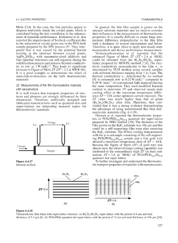
Harman et al. reported the thermoelectric proper-
ties of PbTe/PbTe 0.02 Se 0.98 quantum dot super-lattice
Voltage T.C. prepared by MBE method [10]. The thickness of the
T.C. film grown on the BaF substrate was 104 m and this
2
could be a self-supporting film even after removing
the BaF substrate. The Peltier cooling demonstration
2
with the p–n unicouple consisting of the self-support-
ing PbTe/PbTe 0.02 Se 0.98 sample and a fine gold wire
showed a maximum temperature drop of T 44K.
Because the Figure of Merit (ZT) of gold wire was
Current
almost zero, the observed large cooling capability was
Sample attributed to the extraordinary high ZT (in their esti-
mation ZT 1.6 at 300K) of PbTe/PbTe 0.02 Se 0.98
quantum dot super-lattice.
Figure 6.4.17 To further investigate and understand the thermoelec-
Harman method. tric transport properties of materials with nanostructures,
Figure 6.4.18
Thermoelectric thin films with super-lattice structure. (a) Bi Te /Sb Te super-lattice with the period of 6 nm and total
3
2
3
2
thickness of 5.4 m [8]. (b) PbTe/PbSe quantum dot super-lattice with the period of 13 nm and total thickness of 104 m [10].
357