
Page 478 - Book Hosokawa Nanoparticle Technology Handbook
P. 478
APPLICATIONS 7 FORMATION OF THICK ELECTRONIC CERAMIC FILMS
[48] H. Li, J.H. Song, J.S. Park and K. Han: Int. J. Pharm., [51] J. Du, S. Zhang, R. Sun, L.F. Zhang, C.D. Xiong and
258, 11–19 (2003). Y.X. Peng: J. Biomed. Mater. Res., 72B, 299–304 (2005).
[49] M.S. Mesiha, M.B. Sidhom and B. Fasipe: Int. [52] M.G. Fuentes, D. Torres and M.J. Alonso: Int. J. Pharm.,
J. Pharm., 288, 289–293 (2005). 296, 122–132 (2005).
[50] A.C. Foss, T. Goto, M. Morishita and N.A. Peppas: [53] K.H. Song, S.J. Chung and C.K. Shim: J. Control.
Eur. J. Pharm. Biopharm., 57, 163–169 (2004). Release, 106, 298–308 (2005).
APPLICATION 7
7 FORMATION OF THICK ELECTRONIC CERAMIC FILMS WITH BONDING
TECHNIQUE OF CRYSTALLINE FINE PARTICLES AND THEIR APPLICATIONS
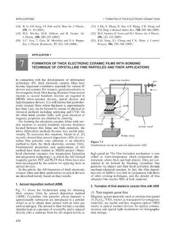
In connection with the developments of information deposition chamber gas
technology (IT), thick electronic ceramic films have
become important constitutive materials for various IT nozzle
devices and systems. For instance, good piezoelectric or
ferromagnetic thick films having thickness from several
microns to several hundreds microns are required in
MEMS micro-actuator devices, optical devices and
high-frequency devices. It is well known that good elec-
tronic ceramic films whose thickness is approximately mask
less than 1 m can be formed by means of physical or
chemical methods including sputtering and CVD. On
the other hand, ceramic bulks with good electrical or
magnetic properties are obtained by sintering. film
For forming the electronic ceramic films with sev-
eral microns to several hundreds microns thickness substrate powder vessel
located between thin films and bulk materials, the
above fabrication methods become less useful unfa-
vorably. To overcome this situation, Akedo et al. [1] Rotary pump
recently showed that aerosol deposition (AD) of crys-
talline fine particles onto substrate is an effective Figure 7.1
method to form the thick electronic ceramic films. Fundamental set-up for aerosol deposition (AD).
Fundamental properties and applications of AD
method have been studied as NEDO project (Nano-
level electronic ceramics low temperature formation high-speed jet. The film formation mechanism is now
and integration technology), in which the AD-formed called as room-temperature shock-compaction phe-
magnetic garnet, PZT and PLZT thick films have also nomenon, where thick and high-density films are con-
been investigated by the authors for applying them in sidered to be formed by breaking crystalline fine
optical devices. particles via impact and their local activation through
In this article, the AD formation of thick electronic mechano-chemical reaction. In fact, the film deposi-
ceramic films and their applications in optical devices tion rate of ADM is very fast in comparison with those
are described mostly based on their results. of other existing techniques, and the density of thus
obtained film reaches 90% of bulk materials.
1. Aerosol deposition method (ADM)
2. Formation of thick electronic ceramic films with ADM
Fig. 7.1 shows the fundamental setup for obtaining
thick ceramic films by aerosol deposition method (1) Thick magnetic garnet films
(ADM). Crystalline fine particles whose diameter is Magnetic garnet materials such as yttrium iron garnet
approximately submicron are introduced in a powder (Y Fe O ; YIG), known as transparent ferromagnetic
5
3
12
vessel so as to obtain their aerosol with an inert gas materials, are useful and key magneto-optical (MO)
such as nitrogen. The aerosol is then led into a vacuum media in optical isolator devices for optical commu-
chamber kept at a pressure of several Pa, and is sprayed nication and spatial light modulators for holographic
directly onto a substrate from the slit-shaped nozzle as data storage.
450