
Page 479 - Book Hosokawa Nanoparticle Technology Handbook
P. 479
7 FORMATION OF THICK ELECTRONIC CERAMIC FILMS APPLICATIONS
0.4
0.2 0
Faraday rotation F (deg/Hm) -0.4
-0.2
-0.6
1 μm -0.8 before anneal
-1
700 °C 60 min annealed
-1.4
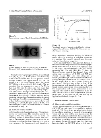
Figure 7.2 -1.2
Cross-sectional image of the AD-formed thick Bi:YIG film. -1.6
400 500 600 700 800 900
Wavelength (nm)
Figure 7.4
Wavelength spectra of magneto-optical Faraday rotation
angles of the AD-formed thick Bi:YIG films before and
after the post annealing.
5 mm
phases was always a problem, because the difference
easily led to the formation of undesired phases and
the resultant film normally showed poor ferromag-
netic and ferroelectric properties.
15 mm
ADM inherently has no such problem because of
the use of crystalline particles whose crystallographic
Figure 7.3
Surface photograph of the AD-formed thick Bi:YIG film. structures are the same as those of the objective films.
The word “YIG” which was placed behind the film is seen. In this respect, the authors fabricated a Bi:YIG/PZT
composite thick film with ADM. Fig. 7.5 shows the
X-ray diffraction chart of thus obtained films, indi-
cating clear coexistence of Bi:YIG and PZT per-
To obtain thick magnetic garnet films, Bi-substituted
YIG (Bi Y Fe O ; Bi:YIG) films were formed by ovskite phases. The film was identified as
ferromagnetic through VSM measurements where the
12
0.5
2.5
5
ADM with crystalline Bi:YIG fine particles whose saturation magnetization of film was similar to that of
average diameter was approximately 500 nm. As Bi:YIG single film. At the moment, ferroelectric
shown in Fig. 7.2, ADM enabled us to form thick properties of film have been studied in detail. If the
Bi:YIG film with considerably high density. The as- ferromagnetism and ferroelectricity are both main-
deposited film was transparent as seen in Fig. 7.3. In tained at room temperature, strong coupling between
this case, the film deposition rate was more than the magnetization and electric polarization is also
1 m/min, which is very fast and satisfactory for prac- expected. This kind of thick multiferroic films are
tical applications, although the crystallographic struc- very attractive because the magnetization (electric
ture of thus obtained films was found to be deteriorated polarization) of the film can be controlled by the
from that of the starting Bi:YIG fine particles, mainly application of electric (magnetic) field.
due to the introduction of strains through the impact of
fine particles. Favorably, such strains could be released
and crystallographic structure was recovered after post 3. Applications of AD ceramic films
annealing. As a result, the post-annealed Bi:YIG film
showed magneto-optical responses similar to those of (1) Magneto-optic spatial light modulators
sputtered films (Fig. 7.4). A novel type of magneto-optic spatial light modulators
(MOSLM) are now under investigation by utilizing
(2) Multiferroic ceramic thick films thick AD PZT films. SLMs are optical micro-devices
ADM enables us to form thick ceramic films at a rel- for modulating amplitude or phase of traveling optical
atively low temperature. This leads to a natural con- waves, and are now widely used in projectors, for
sequence that the technique will be useful for instance. Recently, associated with the developments of
obtaining composite multiferroic ceramic films, mix- holographic memory, SLMs with faster operation speed
ture of ferromagnetic and ferroelectric materials. To are required for ensuring the high data transfer speed of
obtain such a composite film, difference in formation the memory. To meet the requirements, the authors have
temperatures of the ferromagnetic and ferroelectric been developing the MOSLM, where optical wave is
451