
Page 480 - Book Hosokawa Nanoparticle Technology Handbook
P. 480
APPLICATIONS 7 FORMATION OF THICK ELECTRONIC CERAMIC FILMS
G
YIG
YI
PZT
PZT
n
eal
ed
Annealed
A
n
Intensity (A.U.) Intensity (A.U.) A s-fo r med
°
C
at 500
at 500 °C
As-formed
Powder
Po wd er
20 25 30 35 40 45
20
45
25
30
40
35
2 2 (deg)
g)
(de
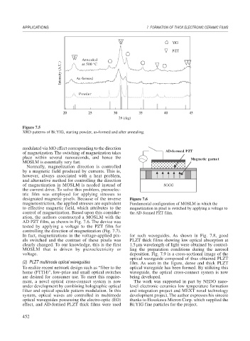
Figure 7.5
XRD patterns of Bi:YIG, starting powder, as-formed and after annealing.
modulated via MO effect corresponding to the direction
of magnetization. The switching of magnetization takes AD-formed PZT
place within several nanoseconds, and hence the Magnetic garnet
MOSLM is essentially very fast.
Normally, magnetization direction is controlled
by a magnetic field produced by currents. This is,
however, always associated with a heat problem,
and alternative method for controlling the direction
of magnetization in MOSLM is needed instead of SGGG
the current drive. To solve this problem, piezoelec-
tric film was employed for applying stresses to
designated magnetic pixels. Because of the inverse Figure 7.6
magnetostriction, the applied stresses are equivalent Fundamental configuration of MOSLM in which the
to effective magnetic field, which attributes to the magnetization in pixel is switched by applying a voltage to
control of magnetization. Based upon this consider- the AD-formed PZT film.
ation, the authors constructed a MOSLM with the
AD PZT film, as shown in Fig. 7.6. The device was
tested by applying a voltage to the PZT film for
controlling the direction of magnetization (Fig. 7.7).
In fact, magnetizations in the voltage-applied pix- for such waveguides. As shown in Fig. 7.8, good
els switched and the contrast of these pixels was PLZT thick films showing low optical absorption at
clearly changed. To our knowledge, this is the first 1.5 m wavelength of light were obtained by control-
MOSLM that is driven by piezoelectricity or ling the preparation conditions during the aerosol
voltage. deposition. Fig. 7.9 is a cross-sectional image of the
optical waveguide composed of thus obtained PLZT
(2) PLZT multimode optical waveguides film. As seen in the figure, dense and thick PLZT
To realize recent network design such as “fiber to the optical waveguide has been formed. By utilizing this
home (FTTH)”, low-price and small optical switches waveguide, the optical cross-connect system is now
are desired for consumer use. To meet this require- being developed.
ment, a novel optical cross-connect system is now The work was supported in part by NEDO nano-
under development by combining holographic optical level electronic ceramics low temperature formation
filter and optical speckle pattern modulation. In this and integration project and MEXT novel technology
system, optical waves are controlled in multimode development project. The author expresses his sincere
optical waveguides possessing the electro-optic (EO) thanks to Hosokawa Micron Corp. which supplied the
effect, and AD-formed PLZT thick films were used Bi:YIG fine particles for the project.
452