Page 105 - Op Amps Design, Applications, and Troubleshooting
P. 105
88     AMPLIFIERS


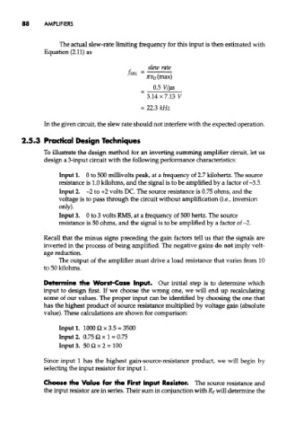
                    The actual slew-rate limiting frequency for this input is then estimated with
               Equation (2.11) as


               In the given circuit, the slew rate should not interfere with the expected operation.

        2.5.3 Practical Design Techniques
               To illustrate the design method for an inverting summing amplifier circuit, let us
               design a 3-input circuit with the following performance characteristics:

                    Input 1. 0 to 500 millivolts peak, at a frequency of 2.7 kilohertz. The source
                    resistance is 1.0 kilohms, and the signal is to be amplified by a factor of -3.5.
                    Input 2. -2 to +2 volts DC. The source resistance is 0.75 ohms, and the
                    voltage is to pass through the circuit without amplification (i.e., inversion
                    only).
                    Input 3. 0 to 3 volts RMS, at a frequency of 500 hertz. The source
                    resistance is 50 ohms, and the signal is to be amplified by a factor of -2.

               Recall that the minus signs preceding the gain factors tell us that the signals are
               inverted in the process of being amplified. The negative gains do not imply volt-
               age reduction.
                    The output of the amplifier must drive a load resistance that varies from 10
               to 50 kilohms.

               Determine the Worst-Case Input. Our initial step is to determine which
               input to design first. If we choose the wrong one, we will end up recalculating
               some of our values. The proper input can be identified by choosing the one that
               has the highest product of source resistance multiplied by voltage gain (absolute
               value). These calculations are shown for comparison:

                    Input 1. 10000x3.5 = 3500
                    Input2. 0.750x1 = 0.75
                    Inputs. 500x2 = 100

               Since input 1 has the highest gain-source-resistance product, we will begin by
               selecting the input resistor for input I.

               Choose the Value for the First Input Resistor. The source resistance and
               the input resistor are in series. Their sum in conjunction with R F will determine the

