
Page 109 - Op Amps Design, Applications, and Troubleshooting
P. 109
AMPLIFIERS
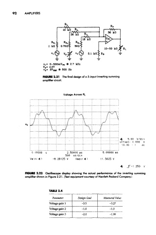
FIGURE 2.21 The final design of a 3-input inverting summing
amplifier circuit.
Voltage Across R L
4 _f~-1.250 V
FIGURE 2.22 Oscilloscope display showing the actual performance of the inverting summing
amplifier shown in Figure 2.21. {Test equipment courtesy of Hewlett-Packard Company.)
TABLE 2.4
Parameter Design Goal Measured Value
Voltage gain 1 -3.5 -3.27
Voltage gain 2 -1.0 -1.0
Voltage gain 3 -2.0 -1.99