Page 108 - Op Amps Design, Applications, and Troubleshooting
P. 108
Inverting Summing Amplifier  91


         The worst-case output will be

                         i? o(max) = i; Ol(max) + u O2(max) + v 03(max)
                                 = (-1.75 V) + (-2 V) + (-8.48 V]
                                 = -12.2 V


             Unless the internal drop on the output of the selected op amp is unusually
         high, we should be able to use standard ±15-volt supplies. Suppose, for example,
         we decide to use a 741 op amp. The manufacturer's data sheet in Appendix 1 indi-
         cates that the op amp can deliver at least ±12 volts to a load >10 kilohms when
         ±15-volt supplies are used. We will plan to use a 741 unless we encounter prob-
         lems with bandwidth or slew rate (verified in subsequent sections).

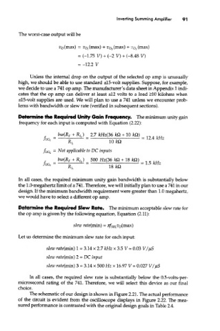
         Determine the Required Unify Gain Frequency. The minimum unity gain
         frequency for each input is computed with Equation (2.22):


        In all cases, the required minimum unity gain bandwidth is substantially below
        the 1.0-megahertz limit of a 741. Therefore, we will initially plan to use a 741 in our
        design. If the minimum bandwidth requirement were greater than 1.0 megahertz,
        we would have to select a different op amp.

        Determine the Required Slew Rote. The minimum acceptable slew rate for
        the op amp is given by the following equation, Equation (2.11):

                               slew rate(min) = jf SRLv 0(max)

        Let us determine the minimum slew rate for each input:

                    slew mte(mm) 1 = 3.14 x 2.7 kHz x 3.5 V = 0.03 VIpS

                    slew rate(min) 2 = DC input
                    slew nzte(min) 3 = 3.14 x 500 Hz x 16.97 V = 0.027 V/j/S

             In all cases, the required slew rate is substantially below the 0.5-volts-per-
        mkrosecond rating of the 741. Therefore, we will select this device as our final
        choice.
             The schematic of our design is shown in Figure 2.21. The actual performance
        of the circuit is evident from the oscilloscope displays in Figure 2.22. The mea-
        sured performance is contrasted with the original design goals in Table 2.4.

