Page 155 - Op Amps Design, Applications, and Troubleshooting
P. 155
138    VOLTAGE COMPARATORS


                 3. Input reference           0 volts
                 4. Minimum output voltage    ±10 volts
                 5. Load resistance           68 kilohms


               Op Amp Selection. We must select an op amp that can satisfy the output
               voltage requirements, survive the input voltage swings, and respond to the
               input frequencies. The manufacturer's data sheet in Appendix 1 confirms that a
               741 is capable of delivering a ±10-volt output. More specifically, the minimum
               output voltage with ±15-volt supplies and a load of greater than 10 kilohms is
               ±12 volts.
                    Additionally, the data sheet indicates that input voltage levels may be as
               high as the value of supply voltage. So far, the 741 seems like a good choice. Now
               let us consider the frequency effects.
                    The open-loop voltage comparator application requires the output voltage
               of the op amp to change from one extreme to the other. This change requires a
               finite amount of time. For DC or low-frequency applications, this amount of
               time is generally insignificant. As the input frequency increases, however, the
               switching time becomes a greater portion of the total time for one alternation of
               the input signal. In the extreme case, if the input alternation were shorter than
               the time required for the output to change states, then the comparator would
               cease to function properly. That is, the output voltage would not have time to
               reach its limits.
                    The slew rate of the op amp determines the maximum rate of change in the
               output voltage. The minimum acceptable rate of change is determined by the
               application. For purposes of example and as a good rule of thumb, let us design
               our circuit to have rise and fall times of no greater than 10 percent of the time for
               an alternation of the input signal. For our present design, the highest input fre-
               quency was specified as 10 kilohertz. The time for one alternation can be calcu-
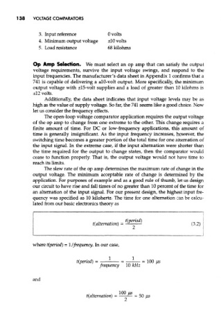
               lated from our basic electronics theory as


               where t(period) = 1 /frequency. In our case,


               and

