
Page 269 - Op Amps Design, Applications, and Troubleshooting
P. 269
Voltage Regulation Fundamentals 251
The second percentage, called load regulation, provides an indication of the regula-
tor's ability to compensate for changes in load current. It is computed as
„. . , , . V REG(no load) - V REG(full load) ^ nn
% load regulation = -^ ^^ x 100
VgEcfoll load)
6.1.5 Voltage References
All of the regulator circuits described in this chapter require a stable reference
voltage. The actual load voltage is continuously compared against this reference
to determine what changes are required by the regulator circuit. In essence, the
voltage reference is in itself a voltage regulator circuit.
Although a zener diode is a low-cost, practical reference source, the actual
zener voltage changes significantly with changes in current through the zener.
Therefore, if we want a more stable source, we must go beyond the simple zener
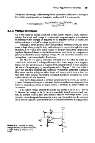
regulator. Figure 6.5 shows a circuit that combines a zener diode and an op amp to
produce a simple but stable reference voltage. We will utilize this circuit in all of
the regulator circuits described in this chapter.
The MC3401 op amp is somewhat different than the other op amps dis-
cussed so far in the text. It is designed for operation from a single power supply—
that is, only one power source is required for normal operation. A more complete
discussion of single-supply op amps is presented in Chapter 11. For now, suffice it
to say that the input terminals are essentially PN junctions connected to ground.
This means that the voltage on either input will remain at 0.6 volts or less. You
may think of the input as responding to current changes in the same way as the
emitter-base circuit of a transistor.
Since the voltage across RI is constant (approximately 0.6 volts), its current is
constant. It is essentially equal to the zener diode current because the op amp bias
current is insignificant. Since the zener current is constant, the zener voltage will
be constant.
If the output voltage attempts to change, this change is felt on the (-) pin via
Dj. Because the voltage on the (-) input is essentially limited by an internal junc-
tion, the changes fed back have only minimal effect on the voltage on the (-) pin,
but rather cause changes in bias currents. In any case, the result is that the output of
the op amp changes in a polarity that tends to compensate for the changing output
FIGURE 6.5 A simple, but stable,
voltage reference can be built around
a single-supply op amp and zener
diode.