
Page 274 - Op Amps Design, Applications, and Troubleshooting
P. 274
256 POWER SUPPLY CIRCUITS
TABLE 6.1
Design Goal Measured Value
Input voltage (DC) +10-15 volts +10-15 volts
Output voltage (V REF) +4 volts +3.985 volts
Percent regulation 0.1 percent 0.004 percent
Reference current 0-1 milliamperes 0-1 milliamperes
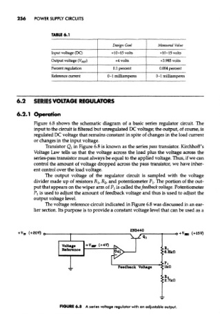
6.2 SERIES VOLTAGE REGULATORS
6*2.1 Operation
Figure 6.8 shows the schematic diagram of a basic series regulator circuit. The
input to the circuit is filtered but unregulated DC voltage; the output, of course, is
regulated DC voltage that remains constant in spite of changes in the load current
or changes in the input voltage.
Transistor Q l in Figure 6.8 is known as the series pass transistor. Kirchhoff's
Voltage Law tells us that the voltage across the load plus the voltage across the
series-pass transistor must always be equal to the applied voltage. Thus, if we can
control the amount of voltage dropped across the pass transistor, we have inher-
ent control over the load voltage.
The output voltage of the regulator circuit is sampled with the voltage
divider made up of resistors RI, R 2, and potentiometer Pj. The portion of the out-
put that appears on the wiper arm of PI is called the feedback voltage. Potentiometer
PI is used to adjust the amount of feedback voltage and thus is used to adjust the
output voltage level.
The voltage reference circuit indicated in Figure 6.8 was discussed in an ear-
lier section. Its purpose is to provide a constant voltage level that can be used as a
+VH (+2QV) 0
FIGURE 6.8 A series voltage regulator with an adjustable output.