
Page 277 - Op Amps Design, Applications, and Troubleshooting
P. 277
Series Voltage Regulators 259
Whichever of these limitations is reached first will determine the maximum allow-
able current that can be drawn from the regulator output
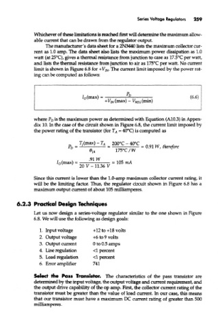
The manufacturer's data sheet for a 2N3440 lists the maximum collector cur-
rent as 1.0 amp. The data sheet also lists the maximum power dissipation as 1.0
watt (at 25°C) / gives a thermal resistance from junction to case as 17.5°C per watt,
and lists the thermal resistance from junction to air as 175°C per watt. No current
limit is shown in Figure 6.8 for +1/V The current limit imposed by the power rat-
ing can be computed as follows:
where P D is the maximum power as determined with Equation (A10.3) in Appen-
dix 10. In the case of the circuit shown in Figure 6.8, the current limit imposed by
the power rating of the transistor (for T^ = 40°C) is computed as
Since this current is lower than the 1.0-amp maximum collector current rating, it
will be the limiting factor. Thus, the regulator circuit shown in Figure 6.8 has a
maximum output current of about 105 milliamperes.
6.2.3 Practical Design Techniques
Let us now design a series-voltage regulator similar to the one shown in Figure
6.8. We will use the following as design goals:
1. Input voltage +12 to +18 volts
2. Output voltage +6 to 9 volts
3. Output current 0 to 0.5 amps
4. Line regulation <1 percent
5. Load regulation <1 percent
6. Error amplifier 741
Select the Pass Transistor. The characteristics of the pass transistor are
determined by the input voltage, the output voltage and current requirement, and
the output drive capability of the op amp. First, the collector current rating of the
transistor must be greater than the value of load current. In our case, this means
that our transistor must have a maximum DC current rating of greater than 500
milliamperes.