Page 276 - Op Amps Design, Applications, and Troubleshooting
P. 276
258     POWER SUPPLY CIRCUITS


                move the wiper arm down, we reduce the amount of feedback voltage (le., less
                positive), increase the bias on Qj, decrease the voltage drop across Q 1; and cause
                the load voltage to increase to a higher regulated level.
                    It is important to note that the series-regulator circuit shown in Figure 6.8 is
                not immune to short circuits. That is, if the output of the regulator was acciden-
                tally shorted to ground, the pass transistor would undoubtedly be destroyed by
                the resulting Wgh-current flow. Many, if not most, regulated supplies are designed
                to be current limited. Section 6.5 discusses this option in greater detail.


        6.2.2 Numerical Analysis

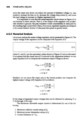
                Let us now analyze the series-voltage regulator circuit presented in Figure 6.8. The
                output voltage of the regulator can be computed with Equation (6.5),


                               are  e
                where RI and R 2   *h  equivalent values shown in Figure 6.9 and as discussed.
                If we assume that the wiper arm of Fj is moved to the uppermost extreme, we can
                apply Equation (6.5) to compute the minimum output voltage as shown:


               Similarly, we can move the wiper arm to the lowest position and compute the
               highest output voltage with Equation (6.5) as follows:


               So the range of regulated output voltages that can be obtained by adjusting P } is
                11.36 through 15.56 volts.
                    The maximum allowable output current is determined by one of the fol-
               lowing:

                  1. Maximum collector current rating of Qj
                  2. Maximum power dissipation rating of Q l
                  3. Current limitation of + V IN

