
Page 275 - Op Amps Design, Applications, and Troubleshooting
P. 275
Series Voltage Regulators 257
stable reference. The schematic of a representative voltage reference circuit was
presented in Figure 6.5.
The op amp in Figure 6.8 is called the error amplifier. It continuously com-
pares the magnitude of the reference voltage with the level of the feedback signal
(which represents the output voltage). Any difference between these two voltages
(both magnitude and polarity) is amplified and applied to the base of the pass
transistor. The polarity is such that the output voltage is returned to its correct
value. As an example, let us assume that the load current suddenly decreases,
which tends to make the output voltage rise. However, as soon as the output volt-
age starts to increase (i.e., become more positive), the feedback voltage on the
wiper arm of P t also becomes more positive. This increasing positive on the
inverting pin of the op amp causes the output of the op amp to become less posi-
tive (i.e., moves in the negative direction). Recall that the reference voltage
remains constant, so any changes in the feedback voltage are immediately
reflected in the output of the op amp. This reduced positive voltage on the base of
Qi reduces the amount of forward bias and therefore increases the effective resis-
tance of the pass transistor, causing an increased voltage drop across it. Because
we are now dropping more voltage across the pass transistor, we will have less
dropped across the load (Klrchhoff's Voltage Law). Thus, the initial tendency for
the load voltage to rise has been offset by an increased voltage drop across the
pass transistor. This process happens nearly instantaneously so that the load volt-
age never really sees a significant increase. Of course, the better the degree of reg-
ulation, the smaller the changes in load voltage.
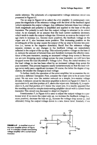
To further clarify the operation of the error amplifier, let us examine the cir-
cuit from a different viewpoint. First, consider the wiper arm to be at some fixed
point. We can now view the resistor network as a simple, two-resistor voltage
divider. A redrawn circuit for the error amplifier is shown in Figure 6.9. Here R{ is
equivalent to R t and that portion of PI above the wiper arm. Similarly, K 2 is equiv-
alent to R 2 and that portion of PI below the wiper arm. It is readily apparent that
the resulting circuit is a simple noninverting amplifier circuit with a current boost
transistor. This circuit was discussed in detail in Chapter 2.
Potentiometer PI in Figure 6.8 is used to adjust the output voltage to a par-
ticular level If we move the wiper arm up, we increase the feedback voltage (i.e.,
more positive), decrease the bias on Qi, increase the voltage drop across Q y and
ultimately bring the output voltage down to a new, lower level Similarly, if we
FIGURE 6.9 A simplified circuit of
the error amplifier portion of Figure - «, -=- „
6.8. It is actually a simple noninverting I *
voltage amplifier with a current boost J
transistor. •mitn mi •—**•
ApwaMflKiM&jh —