
Page 272 - Op Amps Design, Applications, and Troubleshooting
P. 272
2S4 POWER SUPPLY CIRCUITS
This, of course, is not a challenging goal. In fact, if the actual zener current were
less than 5 milliamps, we could omit Qi from the design.
The power dissipation for Qi can be estimated with Equation (6.3) as
Finally, Qi must be able to handle the combined currents of J z and I REF as collector
current. In our particular case,
Let us choose a common 2N2222A as the current booster for our design. The data
sheet in Appendix 3 indicates that it will exceed our requirements. By following
the process presented in Appendix 10, we can determine that no heat sink will be
necessary, but the transistor will operate fairly hot. It might be desirable to add a
small heat sink.
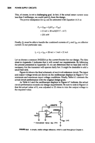
Figure 6.6 shows the final schematic of our 4-volt reference circuit. The input
and output voltage levels are shown on the oscilloscope displays in Figure 6.7 for
minimum and maximum input voltage conditions. Finally, Table 6.1 contrasts the
actual circuit performance with the original design goals.
As Table 6.1 and the oscilloscope displays in Figure 6.7 indicate, the actual
circuit performance exceeds our design i^uirements. Be sure to note in Figure 6.6
that the actual value of Rj was adjusted to 22 ohms to trim the output voltage to
the required value.
FIGURE 6.6 A simple, stable voltage reference, which is used throughout Chapter 6.