Page 271 - Op Amps Design, Applications, and Troubleshooting
P. 271
Voltage Regulation Fundamentals  253


              Let us now design a voltage reference to be used as a stable source for the
         regulator circuits presented in this chapter. We use the following design goals:


           1. Unregulated input voltage   +10 to 15 volts DC
           2. Regulated output voltage    +4 volts
           3. Percent of voltage regulation  0.1 percent
           4. Maximum reference current   1 milliampere


         Choose 0j • The required voltage for DI can be determined by applying Equa-
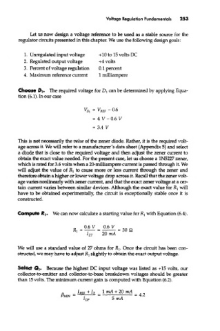
         tion (6.1). In our case


         This is not necessarily the value of the zener diode. Rather, it is the required volt-
         age across it. We will refer to a manufacturer's data sheet (Appendix 5) and select
         a diode that is dose to the required voltage and then adjust the zener current to
         obtain the exact value needed. For the present case, let us choose a 1N5227 zener,
         which is rated for 3.6 volts when a 20-mUliampere current is passed through it. We
        will adjust the value of RI to cause more or less current through the zener and
         therefore obtain a higher or lower voltage drop across it. Recall that the zener volt-
         age varies nonlinearly with zener current, and that the exact zener voltage at a cer-
        tain current varies between similar devices. Although the exact value for RI will
        have to be obtained experimentally, the circuit is exceptionally stable once it is
        constructed.


        Compute RI . We can now calculate a starting value for RI with Equation (6.4).


        We will use a standard value of 27 ohms for R T. Once the circuit has been con-
        structed, we may have to adjust RI slightly to obtain the exact output voltage.


        Select Of. Because the highest DC input voltage was listed as +15 volts, our
        collector-to-emitter and collector-to-base breakdown voltages should be greater
        than 15 volts. The minimum current gain is computed with Equation (6.2).

