
Page 402 - Op Amps Design, Applications, and Troubleshooting
P. 402
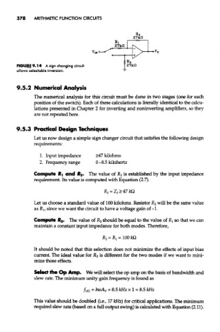
378    ARITHMETIC FUNCTION CIRCUITS


        FIGURE 9.14 A sign changing circuit
        allows selectable inversion.


        9.5.2 Numerical Analysis
               The numerical analysis for this circuit must be done in two stages (one for each
               position of the switch). Each of these calculations is literally identical to the calcu-
               lations presented in Chapter 2 for inverting and noninverting amplifiers, so they
               are not repeated here.


        9.5.3 Practical Design Techniques

               Let us now design a simple sign changer circuit that satisfies the following design
               requirements:

                  1. Input impedance     >47 kilohms
                  2. Frequency range     0-8.5 kilohertz

               Compute JRi and R*. The value of Rj is established by the input impedance
               requirement. Its value is computed with Equation (2.7).


               Let us choose a standard value of 100 kilohms. Resistor R 2 will be the same value
               as RI, since we want the circuit to have a voltage gain of -1.

               Compute R 3. The value of R 3 should be equal to the value of Rj so that we can
               maintain a constant input impedance for both modes. Therefore,


               It should be noted that this selection does not minimize the effects of input bias
               current. The ideal value for JR 3 is different for the two modes if we want to mini-
               mize those effects.

               Select the Op Amp. We will select the op amp on the basis of bandwidth and
               slew rate. The minimum unity gain frequency is found as


               This value should be doubled (ie., 17 kHz) for critical applications. The minimum
               required slew rate (based on a full output swing) is calculated with Equation (2.11).