Page 399 - Op Amps Design, Applications, and Troubleshooting
P. 399
Absolute Value Circuit  375


               For negative input voltages, the output is equal in amplitude but opposite in
               polarity. This, coupled with our previous analysis for positive input voltages,
               means that the output voltage is positive for either polarity of input voltage and
               equal in amplitude to the input voltage. Of course, this is the proper behavior for
               an absolute value circuit where V^ = I Vj I.
                    The input impedance, output impedance, frequency response, and so on, are
               computed in the same manner as are similar circuits previously discussed in
               detail. These calculations are not repeated here,


        9.4.3 Practical Design Techniques
               Since all resistor values are the same in the absolute value circuit, the calculations
               for design are fairly straightforward. Let us design an absolute value circuit that
               will perform according to the following design goals:

                  1. Input voltage       -10 volts < V } < 10 volts
                  2. Input impedance     >18kilohms
                  3. Frequency range     0 to 100 kilohertz
               Select the Value for R. The minimum value for all of the resistors is deter-
               mined by the required input impedance. The maximum value is limited by the
               nonideal characteristics of the circuit (refer to Chapter 10), but is generally below
               100 kilohms. The minimum value for R can be found by applying Equation (2.7).

                                       R = input impedance = 18 kQ.

               Let us choose to use 22-kilohm resistors for our design.

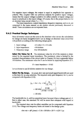
               Select the Op Amps. As usual, slew rate and small signal bandwidth are used
               as the basis for op amp selection. The required unity gain frequency for A 2 can be
               computed with Equation (2.22).


               The bandwidth for AI will be somewhat lower because it has a voltage gain of ~1.
               But in either case, the standard 741 will be more than adequate with regard to
               bandwidth.
                    The required slew rate for either amplifier can be computed with Equation
               (2.11). The voltage and frequency limits are stated in the design goals.

                          slew rate = jijV o(max) = 3.14 x 100 kHz x 20 V = 6.28 V/^Jts

