
Page 394 - Op Amps Design, Applications, and Troubleshooting
P. 394
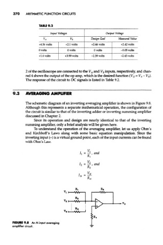
370     ARITHMETIC FUNCTION CIRCUITS


                       TABLE 9.2

                             Input Voltages                  Output Voltage
                         VA              V B        Design Goal     Measured Value
                       +4.56 volts    +2.1 volts    +2.46 volts      +2.42 volts
                       0 volts         0 volts        0 volts        -0.05 volts
                       +1.6 volts     +3.99 volts   -2.39 volts      -2.43 volts


               2 of the oscilloscope are connected to the V A and V B inputs, respectively, and chan-
               nel 4 shows the output of the op amp, which is the desired function (V o - V A - V B).
               The response of the circuit to DC signals is listed in Table 9.2.


        9.3    AVERAGING AMPLIFIER

               The schematic diagram of an inverting averaging amplifier is shown in Figure 9.8.
               Although this represents a separate mathematical operation, the configuration of
               the circuit is similar to that of the inverting adder or inverting summing amplifier
               discussed in Chapter 2.
                    Since its operation and design are nearly identical to that of the inverting
               summing amplifier, only a brief analysis will be given here.
                    To understand the operation of the averaging amplifier, let us apply Ohm's
               and Kirchhoff's Laws along with some basic equation manipulation. Since the
               inverting input (-) is a virtual ground point, each of the input currents can be found
               with Ohm's Law.


        FIGURE 9.8 An N-inpui averaging
        amplifier circuit.