Page 395 - Op Amps Design, Applications, and Troubleshooting
P. 395
Absolute Value Circuit  371


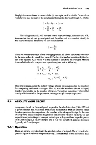
                Negligible current flows in or out of the (-) input pin, so Kirchhoff's Current Law
                will show us that the sum of the input currents must be flowing through R 3, That is,


                    The voltage across K 3 will be equal to the output voltage, since one end of K 3
               is connected to a virtual ground point and the other end is connected directly to
               the output terminal. Therefore, we can conclude that


               Now, for proper operation of the averaging circuit, all of the input resistors must
               be the same value; let us call this value JR. Further, the feedback resistor (R 3) is cho-
               sen to be equal to R/N where N is the number of inputs to be averaged. Making
               these substitutions in our previous equations gives us the following:


               This final expression for the output voltage should be recognized as the equation
               for computing arithmetic averages. That is, add the numbers (input voltages)
               together and divide by the number of inputs. The minus sign simply shows that
               the signal is inverted in the process of passing through the op amp circuit.


        9.4    ABSOLUTE VALUE CIRCUIT

               An op amp circuit can be configured to provide the absolute value (I VALUE 1) of
               a given number. You will recall from basic mathematics that an absolute value
               function produces the magnitude of a number without regard to sign. In the case
               of an op amp circuit designed to generate the absolute value of its input, we can
               expect the output voltage to be equal to the input voltage without regard to polar-
               ity. So, for example, a +6.2-volt input and a -6.2-volt input both produce the same
               (typically +6.2-volt) output.

        9.4.1 Operation

               There are several ways to obtain the absolute value of a signal. The schematic dia-
               gram in Figure 9.9 shows one possible way. The first stage of this circuit is a dual

