
Page 396 - Op Amps Design, Applications, and Troubleshooting
P. 396
372 ARITHMETIC FUNCTION CIRCUITS
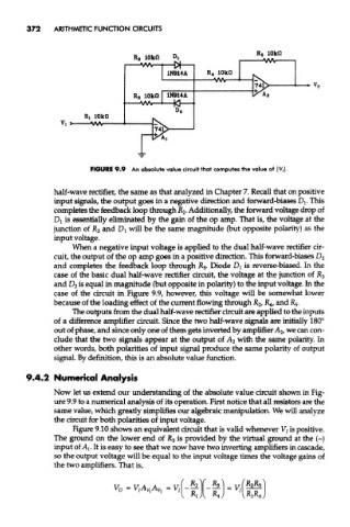
FIGURE 9.9 An absolute value circuit that computes the value of |V,\,
half-wave rectifier, the same as that analyzed in Chapter 7. Recall that on positive
input signals, the output goes in a negative direction and forward-biases DI. This
completes the feedback loop through K 2- Additionally, the forward voltage drop of
D! is essentially eliminated by the gain of the op amp. That is, the voltage at the
junction of R 2 and D l will be the same magnitude (but opposite polarity) as the
input voltage.
When a negative input voltage is applied to the dual half-wave rectifier cir-
cuit, the output of the op amp goes in a positive direction. This forward-biases D 2
and completes the feedback loop through R 3. Diode D! is reverse-biased. In the
case of the basic dual half-wave rectifier circuit, the voltage at the junction of R 3
and D 2 is equal in magnitude (but opposite in polarity) to the input voltage. In the
case of the circuit in Figure 9.9, however, this voltage will be somewhat lower
because of the loading effect of the current flowing through R^ -R^ a^d %
The outputs from the dual half-wave rectifier circuit are applied to the inputs
of a difference amplifier circuit. Since the two half-wave signals are initially 180°
out of phase, and since only one of them gets inverted by amplifier A 2, we can con-
clude that the two signals appear at the output of A 2 with the same polarity. In
other words, both polarities of input signal produce the same polarity of output
signal. By definition, this is an absolute value function.
9*4.2 Numerical Analysis
Now let us extend our understanding of the absolute value circuit shown in Fig-
ure 9.9 to a numerical analysis of its operation. First notice mat all resistors are the
same value, which greatly simplifies our algebraic manipulation. We will analyze
the circuit for both polarities of input voltage.
Figure 9.10 shows an equivalent circuit that is valid whenever Vj is positive.
The ground on the lower end of R 3 is provided by the virtual ground at the (-)
input of A!. It is easy to see that we now have two inverting amplifiers in cascade,
so the output voltage will be equal to the input voltage times the voltage gains of
the two amplifiers. That is,