
Page 389 - Op Amps Design, Applications, and Troubleshooting
P. 389
Adder 365
In our case, we can compute the required value of .R 2 as
R 2 = 5.6 kQ(4 -1) = 16.8 fcQ
If we expect the adder to generate the correct sum, it is essential to keep the resis-
tor ratios correct. Therefore, since 16.8 kilohms is not a standard value, we will
or
need to use a variable resistor for R 2 some combination of fixed resistors (e.g.,
15 kQ in series with 1.8 ifcfl).
Select on Op Amp. There are several nonideal op amp parameters that may
affect the proper operation of the noninverting adder. An op amp should be
selected that irunimizes those characteristics most important for a particular
application. The various nonideal parameters to be considered are discussed in
Chapter 10. In general, if DC signals are to be added, an op amp with a low offset
voltage and low drift will likely be in order. For AC applications, bandwidth and
slew rate are two important limitations to be considered.
Based on the modest gain/bandwidth requirements for this particular appli-
cation, let us use a standard 741 op amp. Other, more precision devices can be sub-
stituted to optimize a particular characteristic (e.g., low noise). Many of these
alternate devices are pin compatible with the basic 741.
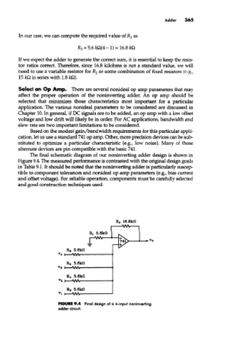
The final schematic diagram of our noninverting adder design is shown in
Figure 9.4. The measured performance is contrasted with the original design goals
in Table 9.1. It should be noted that the noninverting adder is particularly suscep-
tible to component tolerances and nonideal op amp parameters (e.g., bias current
and offset voltage). For reliable operation, components must be carefully selected
and good construction techniques used.
FIGURE 9.4 Final design of a 4-input noninverting
adder circuit.