
Page 410 - Op Amps Design, Applications, and Troubleshooting
P. 410
386 NONIDEAL OP AMP CHARACTERISTICS
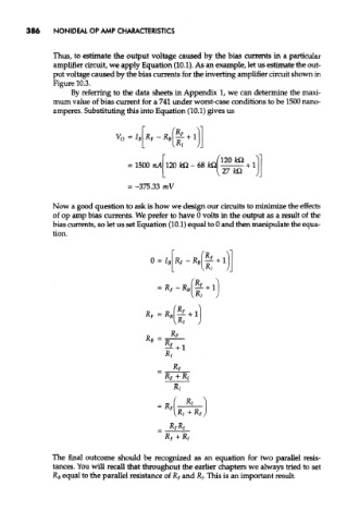
Thus, to estimate the output voltage caused by the bias currents in a particular
amplifier circuit, we apply Equation (10.1). As an example, let us estimate the out-
put voltage caused by the bias currents for the inverting amplifier circuit shown in
Figure 10.3.
By referring to the data sheets in Appendix 1, we can determine the maxi-
mum value of bias current for a 741 under worst-case conditions to be 1500 nano-
amperes. Substituting this into Equation (10.1) gives us
Now a good question to ask is how we design our circuits to minimize the effects
of op amp bias currents. We prefer to have 0 volts in the output as a result of the
bias currents, so let us set Equation (10.1) equal to 0 and then manipulate the equa-
tion.
The final outcome should be recognized as an equation for two paralel resis-
tances. You will recall that throughout the earlier chapters we always tried to set
JR B equal to the parallel resistance of R F and R/. This is an important result.