Page 412 - Op Amps Design, Applications, and Troubleshooting
P. 412
388     NONIDEAL OP AMP CHARACTERISTICS


               The typical values for these currents at room temperature are 20 nanoamperes and
               80 nanoamperes for input offset current and input bias current, respectively.
                    While deriving Equation (10.1), we generated the following intermediate
               step:


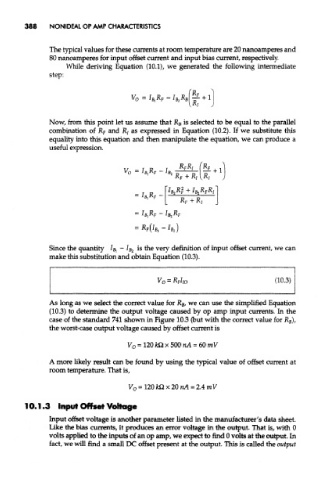
               Now, from this point let us assume that R B is selected to be equal to the parallel
               combination of R F and jR/ as expressed in Equation (10.2). If we substitute this
               equality into this equation and then manipulate the equation, we can produce a
               useful expression.


               Since the quantity l^ - 1% is the very definition of input offset current, we can
               make this substitution and obtain Equation (10.3).


               As long as we select the correct value for R B, we can use the simplified Equation
               (10.3) to determine the output voltage caused by op amp input currents. In the
               case of the standard 741 shown in Figure 10.3 (but with the correct value for R B),
               the worst-case output voltage caused bv offset current is


               A more likely result can be found by using the typical value of offset current at
               room temperature. That is,


        10.1.3 Input Offset Voltage
               Input offset voltage is another parameter listed in the manufacturer's data sheet.
               Like the bias currents, it produces an error voltage in the output. That is, with 0
               volts applied to the inputs of an op amp, we expect to find 0 volts at the output. In
               fact, we will find a small DC offset present at the output. This is called the output

