
Page 415 - Op Amps Design, Applications, and Troubleshooting
P. 415
Nonideal DC Characteristics 391
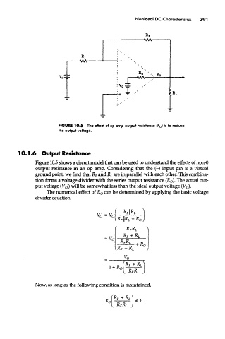
FIGURE 10.5 The effect of op amp output resistance (R 0) is to reduce
the output voltage.
10.1.6 Output Resistance
Figure 10,5 shows a circuit model that can be used to understand the effects of non-0
output resistance in an op amp. Considering that the (-) input pin is a virtual
ground point, we find that R F and R L are in parallel with each other. This combina-
tion forms a voltage divider with the series output resistance (R o). The actual out-
put voltage (V 0') will be somewhat less than the ideal output voltage (V 0).
The numerical effect of R 0 can be determined by applying the basic voltage
divider equation.
Now, as long as the following condition is maintained,