
Page 413 - Op Amps Design, Applications, and Troubleshooting
P. 413
Nonideal DC Characteristics 389
offset voltage and is a result of the combined effects of bias current (previously dis-
cussed above) and input offset voltage.
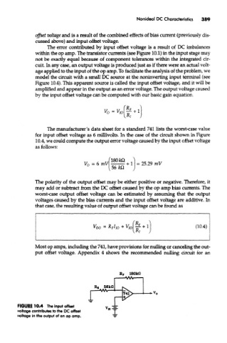
The error contributed by input offset voltage is a result of DC imbalances
within the op amp. The transistor currents (see Figure 10.1) in the input stage may
not be exactly equal because of component tolerances within the integrated cir-
cuit. In any case, an output voltage is produced just as if there were an actual volt-
age applied to the input of the op amp. To facilitate the analysis of the problem, we
model the circuit with a small IX source at the noninverting input terminal (see
Figure 10.4). This apparent source is called the input offset voltage, and it will be
amplified and appear in the output as an error voltage. The output voltage caused
by the input offset voltage can be computed with our basic gain equation.
The manufacturer's data sheet for a standard 741 lists the worst-case value
for input offset voltage as 6 millivolts. In the case of the circuit shown in Figure
10.4, we could compute the output error voltage caused by the input offset voltage
as follows:
The polarity of the output offset may be either positive or negative. Therefore, it
may add or subtract from the DC offset caused by the op amp bias currents. The
worst-case output offset voltage can be estimated by assuming that the output
voltages caused by the bias currents and the input offset voltage are additive. In
that case, the resulting value of output offset voltage can be found as
Most op amps, including the 741, have provisions for nulling or canceling the out-
put offset voltage. Appendix 4 shows the recommended nulling circuit for an
FIGURE 10.4 The input offset
voltage contributes to the DC offset
voltage in the output of an op amp.