
Page 417 - Op Amps Design, Applications, and Troubleshooting
P. 417
Nonideal AC Characteristics 393
The charging current is determined by the design of the op amp and is not con-
trollable by the user. In the case of internally compensated op amps, the value of
capacitance is also fixed. The user does have control over the capacitance values
for externally compensated op amps. The smaller the compensating capacitor, the
wider the bandwidth and the faster the slew rate. Unfortunately, the price paid for
this increased performance is a greater amplification of noise voltages and a
greater tendency for oscillations.
Since slew rate is, by definition, a measure of volts per second, the severity of
problems caused by limited slew rates is affected by both signal amplitude and
signal frequency. We can determine the largest output voltage swing for a given
slew rate and operating frequency by applying Equation (2.11).
Of course, we can also transpose this equation to determine the highest operating
frequency for a given output amplitude.
10.2.3 Noise
The term noise, as used here, refers to undesired voltage (or current) fluctuations
created within the internal stages of the op amp. Although there are many internal
sources of noise, and several types, it is convenient to view the noise sources col-
lectively as a single source connected to the noninverting input terminal. This
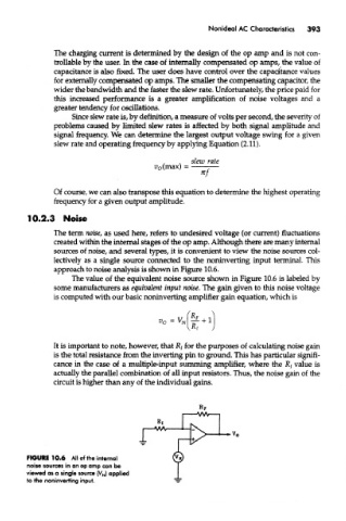
approach to noise analysis is shown in Figure 10.6.
The value of the equivalent noise source shown in Figure 10.6 is labeled by
some manufacturers as equivalent input noise. The gain given to this noise voltage
is computed with our basic noninverting amplifier gain equation, which is
It is important to note, however, that R/ for the purposes of calculating noise gain
is the total resistance from the inverting pin to ground. This has particular signifi-
cance in the case of a multiple-input summing amplifier, where the JR/ value is
actually the parallel combination of all input resistors. Thus, the noise gain of the
circuit is higher than any of the individual gains.
FIGURE 10.6 All of the internal
noise sources in an op amp can be
viewed as a single source (V N) applied
to the noninverting input.